(1)
Phase Frequency Detectors (PFD) are the most important components of Phase Locked Loops (PLLs) which gives an output that is linearly proportional to the phase difference of the reference signal (CKR) and output of VCO (CKF) [8]. PFD has a number of applications in communication systems, wireless sensors, and robotics. Some application are focused on the efficiency or bandwidth, some other on low noise and jitters or it can be its size. In this paper, effect of scaling on a latch based PFD is presented. This paper presents the compassion of various technologies using different channel lengths and is useful to determine which is the best suitable channel length having best characteristics. Various technologies of CMOS are used and the performance is considered on the basis of two parameters-power consumed and delay in output when input is already given. The authors have used Tanner EDA 14.11 version on various technologies.
The tri-state PFDs are usually built with memory elements, and thus, they need a reset signal to clear the memory elements. Several tri-state PFD architectures have been discussed, in previous works, including precharge-type PFD [1], ncPFD [2], and latch- based PFD [3–5]. Among these published PFD topologies, the latch-based PFD is the most commonly used one for its high operation speed, low power consumption, wide input range, and independence to the input duty cycle [3]. Effect of scaling is being discussed in this paper. This paper discusses the effect of scaling on power dissipation, noise and delay. These parameters varies when channel length is changed. The authors have considered four technologies using CMOS: 125 μm, 350 nm, 180 nm, and 100 nm.
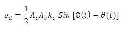
Phase detector can be realized as a multiplier followed by a low pass filter. Multiplier will multiply the input signal xr and output of Voltage control oscillator eo and then the low pass filter filters out unwanted frequencies [6]. When we multiply two signal we will get a sine function of a sum frequency component and a difference frequency component [7-9]. The sum frequency component will be low pass signal filtered out by LPF and the output contains a difference of Ø(t) - θ(t) (insatntaneos phase error).
Let the output of a phase detector is ed (output of LPF), and is given by the equation,
where kd is associated with multiplier.
Latch-based PFD uses two D flip flops which are latched with a NOR gate providing reset signal. When both the inputs are high, the reset signal will force the two inputs to be low so that the PFD can work properly. Extra delay cells are added at the input to provide low jitters and minimal blind zone. In blind zone, the PFD cannot respond to the transitions occurring in this region. For example, if reset is trigged, PFD cannot detect this reset and remains in ON state. Figure 1 shows the block diagram of PD. The circuit diagram of Phase Frequency Detector is shown in Figure 2.
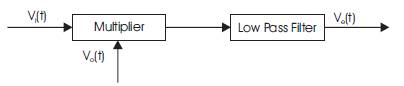
Figure 1. Block Diagram of PD
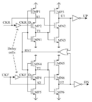
Figure 2. Latch based PFD
Phase Frequency Detector is implemented using Tanner EDA14.11 version using SEDIT, TSPICE, and WEDIT. Implementation is shown in Figure 3.
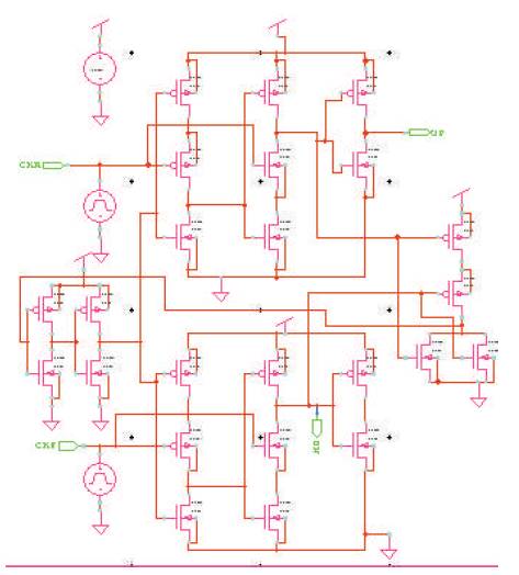
Figure 3. Implementation of PFD with Added Delay Cell
The transient response of PFD with different technologies is being calculated. Transient response of PFD using 125 μm technology is shown in Figure 4.
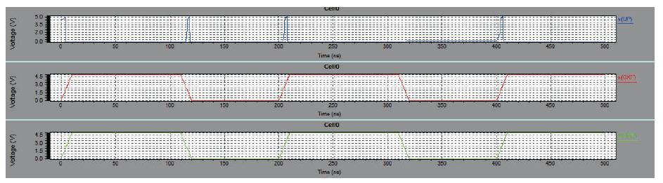
Figure 4. Transient Response at Vdd =5 V using 125 μm Technology
According to definition, PFD will give the output which is linearly proportional to difference in the inputs. In Figure 4, when Two inputs CKR and CKF are in locked state that is CKR and CKF are in phase or synchronized, therefore we can see only transients are coming at rising and falling edges. With this technology, we get the following output for power measurement,
Average power consumed =3.179525e-007 watts
Max power = 6.348412e-003 watts
Min power = 0.000000e+000 watts
Delay measurements are as follows,
Delay = 2.4372e-009sec
Trigger = 2.0000e-009sec
Target = 4.4372e-009sec
In Figure 5, input CKR is leading, therefore the output UP is showing the difference between the two inputs. With this technology we get following output for power measurement,
Average power consumed = 2.959756e-009 watts
Max power = 1.439680e-005 watts
Min power =0.000000e+000 watts
The results for delay are as follows,
Delay = 2.5050e-009sec
Trigger = 2.8571e-009sec
Target = 5.3622e-009sec
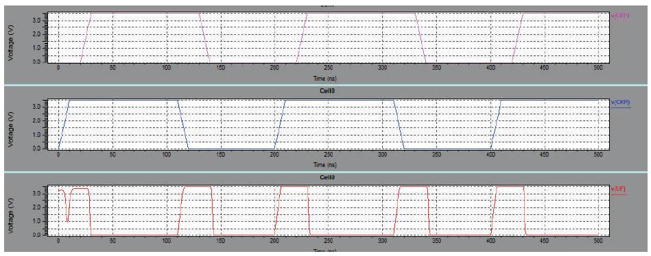
Figure 5. Transient response at Vdd =3.5 V using 350 nm Technology
Figure 6 shows the transient response of PFD using 180 nm technology when PFD is in locked state, that is phase and frequency difference between the input and output are zero.
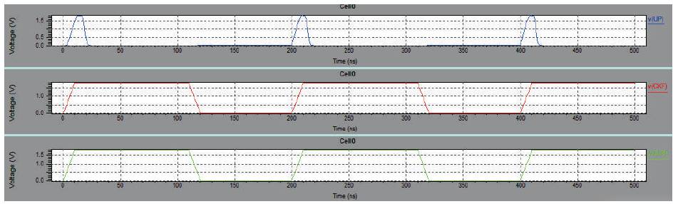
Figure 6. Transient Response at Vdd =1.8 V using 180 nm Technology
With this technology, we get the following output for power measurement,
Average power consumed = 5.164308e-009 watts
Max power = 8.883656e-007watts
Min power =0.000000e+000
Results for delay are as follows,
Delay = 2.3919e-009sec
Trigger = 5.5556e-009sec
Target = 7.9982e-009sec
In Figure 7, PFD is in locked state and the power measurement are as follows,
Average power consumed =6.009589e-010 watts
Max power =1.076263e-007watts
Min power =0.000000e+000
Value of delay measurement are,
Delay = 1.6743e-009sec
Trigger = 8.3333e-009sec
Target = 1.0008e-008 sec
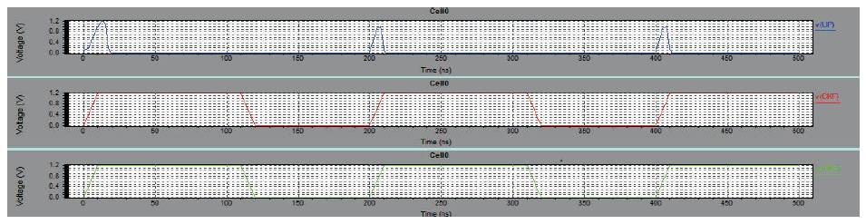
Figure 7. Transient Response at Vdd =1.2 V using 100 nm Technology
Comparison is made on various technologies of CMOS and Power and delay analysis are done (Table 1).

Table 1. Comparison Table for Various CMOS Technologies
Effect of scaling is done using various technologies 125 μm, 350 nm, 180 nm and 100 nm. Based on the above power and delay calculations, we can say that as technology is reduced from 125 μm to 350 nm, the average power is reduced, but there is a slight increase in delay. With decrease from 350 nm to 180 nm, it is observed that the worst case of power increases but delay is reduced further. And in the last case, 100 nm shows the best results of power reduction and minimal delay. In low power applications, we can use 350 nm and 100 nm and for high clocking speed applications in which we require quick response like in robotics, the best scaling technology to use is 100 nm. So, it is concluded that 100 nm technology is best considered among all and can be used in most of the applications.