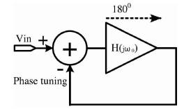
Figure 1. Oscillatory Feedback System
The conventional Voltage-Controlled Oscillators (VCO) are impractical to generate the full swing outputs and wide range of tuning, because the conventional differential VCO's are used as the tail current sources. The full swing, wider tuning range and low voltage VCO's are widely used in every applications. This paper proposes a new CMOS VCO. The proposed VCO uses a single-ended delay cell and achieves the widest tuning range, speed in operation and improved noise performance. The supply voltage used in the proposed system is 1.2V. Moreover, it's simple topology features multiple advantages like area and linear frequency-voltage characteristics. The proposed system has achieved a very wide range of tuning and good noise performance compared to the conventional VCO's. The topology can be used in pulse based applications.
The application of portable devices is popular and important, especially more in communication, medical care [7], [8], and consumer electronic products. Voltage- Controlled Oscillators (VCOs) are widely used in electronic devices to generate a clock or to meet other system demands. For example, the VCOs are the heart of every wired and wireless communication systems, including phase lock loop [9], [10], clock data recovery system [8], digital millimeter, radar, CPU, delay locked loop, and microprocessor-based systems [8]. These subsystem blocks are used in various electronic products. To meet the requirements of portability, electronic products increasingly use low-voltage [15], high Signal-to- Noise Ratio (SNR) monolithic integrated chips. Therefore, an effective design for a low-voltage full-swing on-chip VCO is needed.
The on-chip CMOS VCO technology is typically implemented in ring oscillators and inductor–capacitor (LC) oscillators. Compared with LC structures, the ring structures provide a wider tuning range [16], smaller layout area, lower dissipated power, more output phases, and less design complexity [6]. To achieve high-quality performance in portable device systems at low cost and with a simple design, the ring VCO structures of numerous differential delay cells have been commonly implemented in the recently developed VCO integrated circuits [2] , [3]. However, compared with ring VCOs of single-ended delay cells, implementing ring VCOs of differential delay cells typically requires a larger area [14], greater power consumption, and a tail current circuit. Therefore, determining a method for designing a VCO with a wide tuning range, a simple design with small layout area and high noise performance (without a tail current circuit) is crucial.
Another major concern in VCO design is the variation in the output phase and frequency as a result of noise on the control line [13]. For a given noise amplitude, the noise in the output frequency is proportional to the VCO gain (KVCO) [4], [5]. Thus, the noise on the control line can be reduced by minimizing the KVCO. However, the drawback is a narrow VCO tuning range. The VCO requires a band switch function to reduce noise in the control line and to improve the tuning range [12]. The wider tuned full-swing single-ended delay cell with wide tuning range is a good architecture in the design for VCOs.
The objective of the proposed system is to increase the tuning range and noise performance of the system. The tuning range of the system will increase the selectivity range. The proposed system will have the characteristics of linear frequency- voltage characteristics.
In previous works [1], a single-ended delay cell based even phase VCO was discussed. The VCO can produce the even phase outputs but the tuning range of the VCO is very small, as it is unable to tune wide range of frequencies. A Current Controlled Oscillator (CCO) was developed in [2], which is biased by a constant current, I through MOSFETs. The CCO suffers with high ground bounce problems due to the tail current sources in the circuits. In [3], various convention delay cells developed in the recent years are discussed.
Conventional single-ended ring oscillators using current starved or weighted-current adder inverters provide a low intrinsic phase noise and a high SNR because of their fullswing [11]. However, the conventional single-ended ring oscillators consist of a series of inverting amplifiers placed in a feedback loop and are composed of odd number of inverters. In the previous existed system, the single-ended delay cell is used in implementing four stage symmetrical even phase voltage controlled oscillator [1], but it is suffers with a low tuning range. Most designs use differential ring oscillators. Nevertheless, the single-ended ring VCO is clearly superior in terms of power consumption and noise. Ring oscillators also require a sufficient loop gain to initiate oscillation. Loop gain is usually insufficient in the three-stage ring oscillator. Therefore, the five-phase output ring oscillators with differential delay cells are usually implemented using five-stage architectures that have high power consumption [8]. Compared with conventional differential delay cell topologies, the inverter base ring VCO with the current reuse technique provides a higher amplifier transconductance (gm ) of the VCO without increasing power dissipation. Therefore, the inverter base ring VCO reduces power consumption. Moreover, the inverter base ring VCO technique provides a full-swing output and improves the SNR of the VCO. Figure 1 shows the proposed oscillatory feedback system, and Figure 2 shows the proposed single-ended delay cell circuit. To meet the Barkhausen criterion (H(jω0 ) = 180o ), Figure 1 shows that the proposed ring oscillator has a frequency dependent phase shift of 180° (dashed by the arrow) and a DC phase shift of 180°. Therefore, the phase tuning device Mn1 (in Figure 2) must provide a DC phase shift of 180°. That is, node Vin and node phase tuning must have a 180° phase difference. Moreover, the operating frequency of the proposed VCO can be adjusted by changing ω0 , which is the bandwidth of the proposed delay cell.
Figure 1. Oscillatory Feedback System
The control voltage can be changed to adjust the ONresistance of transistor (Mp3) to achieve proper bandwidth tuning technique. Thus, the output frequency of the VCO can be changed by varying the control voltage. The circuit designer first uses transistors Mn1 and Mp1 to determine the minimum output frequency of a VCO and then uses transistors Mn2 and Mp2 to determine the KVCO. Restated, the gain of the VCO is determined by the transistors Mn2 and Mp2 . In addition, the linear frequency- voltage characteristics can be improved using the transistor Mp3 with a low threshold voltage. This can prevent the transistor (Mp3 ) from being turned OFF too soon. In other words, if the transistor (Mp3 ) is OFF, and Ro Mp3 → ∞, then the output frequency will be small.
The above concepts reveal dependency of how the ONresistance of transistor(Mp3) modify the output frequency. The frequency-voltage characteristics of the proposed VCO are also obtained by tuning the ON-resistance of control transistor (Mp3 ). Therefore, using a low threshold transistor, Mp3 with a voltage control is the best approach is improving the above linear frequency-voltage characteristics. When Mp3 is a p-type transistor, the VCO is operated in frequency tunable states, the ON resistance of Mp3 will be increased as the control voltage increases. The output frequency decreases as the control voltage increases. That is, the proposed VCO circuit has a negative slope. Alternatively, when the system needs a positive change in slope for the VCO, the p-type transistor (Mp3 ) should simply be altered with an n-type frequency p3 tuning state, the Ro Mn3 decreases as the control voltage o n3 increases. The output frequency increases as the control voltage increases. That is, the proposed VCO circuit has a positive slope. In other words, the selected transistor determines whether the linear frequency-voltage relationship of the proposed VCO is positive or negative, which is determined by the transistor nMOS or pMOS.
Figure 2 shows that the proposed single-ended delay cell circuit includes the band switch function circuit and linear frequency-voltage characteristics circuit. The circuit in Figure 2 can be operated in both low- and high-frequency modes. In low-frequency operation, the switch transistors Mn5 and Mp5 are turned OFF. When the proposed VCO is operated in high-frequency, the switch transistors Mn5 and Mp5 are turned ON, and the bandwidth of each stage can be derived. In addition, transistors Mn5 and Mp5 are turned ON concurrently (Ia = Ib , Ia is the current flowing through the transistor Mp5 , Ib is the current flowing through the transistor Mn5. Thus, the bandwidth of the proposed delay cell stage will be increased. Therefore, the output frequency of the VCO is increased when transistors Mn4 and Mp4 are turned ON, and the proposed VCO has a wider tuning range by this band switch function.
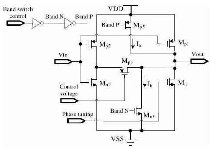
Figure 2. Proposed Single Ended Delay Cell
The proposed VCO structure is shown in Figure 3 and it is similar to the conventional ring topology. The cells illustrated in the topology will be replaced with the proposed single-ended delay cell. The phase tuning to each delay stage will be carried out from the output of the two forward stages. The control voltage applied to the structure will be same for each stage and by controlling the control frequency, we can tune the overall frequency of the structure. The voltage will be dependent on either using pMOS or nMOS as the control transistor.
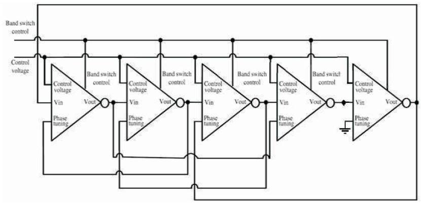
Figure 3. Proposed Five Stage VCO based on Single- ended Delay Cells
The topology is similar to the conventional ring topology. The simple structure will be useful in reducing the overall area of the chip. The output of last stage will be connected back to the input of first stage. The outputs are achieved at the output node of every stage. Figure 4 shows the lower frequency mode when the control voltage is limited to its minimum value and Figure 5 shows the high frequency mode.
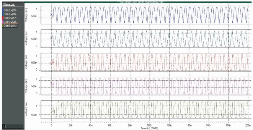
Figure 4. Output Waveform of the Proposed Five Stage VCO Low Frequency Mode
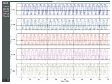
Figure 5. Output Waveform of the Proposed Five Stage VCO High Frequency Mode
In this section, the results obtained for the proposed system are discussed. Figure 4 shows the waveforms of the proposed VCO in low frequency mode. The proposed structure has five stages, so that we can get five outputs. The output frequency of the system in this mode is 111 MHz. Figure 5 is the output of the proposed VCO in high frequency mode. The output frequency of the system is 333 MHz. The output waveforms are oscillating between the voltage levels of 0 V and 1.2 V.
The graph shown in Figure 6 illustrates the frequency variation of the proposed VCO with the controlled voltage. The frequency range is increased with the increase in control voltage. The proposed system has the linear frequency- voltage characteristics. The slope of the curve will be depending on the control transistor. If PMOS is used, the slope will be negative and for NMOS, the slope will be positive. When the control voltage is tuned to its maximum value. The tuning range achieved in the proposed system was 222 MHZ, which it is very high as compared to [1]. The tuning range of the system is improved twice to the existed system. The total delay of any circuit must have a lower value because the total delay of circuit will define the speed of that circuit. The proposed topology also minimizes the total delay compared to the existed system. The noise performance of the system is improved by four percent.
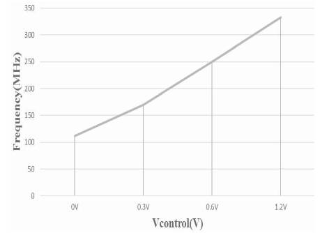
Figure 6. Frequency Change Curve of the Proposed VCO with Control Voltage
The proposed VCO structure is implemented in HSPICE 2008.03 with 180 nm technology that use Avanwaves and HSPICE RF tool for obtaining the total noise of the system. The obtained results are given in Table 1. By comparing the tuning frequency, the proposed system has the wider tuning range over the existed system. The total noise of the system is also improved by a noticeable amount as shown in the comparison Table 1.
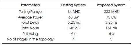
Table 1. Comparison of the Proposed VCO with Existing VCO
In communication, medical care, and consumer electronic applications, full swing and wider tuning range performance are crucial for an effective VCO design. The conventional designs of VCO does not have a wider tuning range and low power simultaneously. However, the implementation of a VCO can be simplified using the proposed single-ended delay cell. Moreover, the proposed delay cell improves the tuning range very effectively and reduces noise in the control line. The noise performance was improved as compared to the previous VCO techniques because of its band switch function and full-swing characteristics. Therefore, the proposed VCO is suitable for communication, medical care, and consumer electronic applications.