Figure 1. Basic Three-Phase Voltage-Source Converter Circuit
This paper deals with the harmonic elimination in multilevel inverters. Multilevel inverters are advanced types of inverters. The desired level of levels is obtained by using the method of triggering. A seven level cascaded H-bridge inverter has been used here. To synthesize multilevel output AC voltage using different levels of DC input, semiconductor devices must be switched on and off. The output contains harmonic and total harmonic distortion. These affect the solution and hence have to be eliminated. Selective harmonic elimination is the method in which the author selects the harmonics which needs to be eliminated. Different methods are used to eliminate the harmonics. In this paper, the author makes use of genetic algorithm to eliminate the harmonics. Genetic algorithm is a computational algorithm that solves optimization problem by imitating the genetic processes and the theory of evolution. It imitates biological evolution by using parameters such as reproduction, crossover mutation etc. The fitness function of multilevel inverters is solved and firing angles are obtained. These firing angles are obtained to the semiconductor devices and output with minimum harmonics and total harmonic distortions are obtained.
Harmonics are electric voltages and currents that appear on the electric power system as a result of certain kinds of electric loads. Harmonic frequencies in the power grid are a frequent cause of power quality problems. Harmonics are the by-products of modern electronics. They occur frequently when there are large numbers of personal computers (Single Phase Loads), Uninterruptible Power Supplies (UPSs), variable frequency drives (AC and DC) or any electronic device using solid state power switching supplies to convert incoming AC to DC. Non-linear loads create harmonics by drawing current in abrupt short pulses, rather than in a smooth sinusoidal manner. The terms “linear” and “non-linear” define the relationship of current to the voltage waveform. A linear relationship exists between the voltage and current, which is typical of an across the line load. A non-linear load has a discontinuous current relationship that does not correspond to the applied voltage waveform. All variable frequency drives cause harmonics due to the nature of the frontend rectifier design. Multilevel inverters are more advanced and latest type of power electronic converters that synthesize a desired output voltage from several levels of dc voltages as inputs. By taking sufficient number of dc sources, a nearly sinusoidal voltage waveform can be synthesized. In comparison with the hard-switched two-level pulse width modulation inverters, multilevel inverters offer several advantages including their capabilities to operate at high voltage with lower voltage stress per switching, high efficiency and low electromagnetic interferences etc. To synthesize multilevel output ac voltage using different levels of dc inputs, semiconductor devices must be switched on and off. The primary objective of this paper is to implement the evolution process of Genetic algorithm to the proposed system and hence eliminating the unwanted harmonics. There are different approaches for the selection of switching techniques for the multilevel inverters; one of the important approaches is Genetic algorithm.
In contrast to grid connected ac motor drives, hardly variable in speed, power electronic devices (e.g., inverter), providing voltage supply variable in both frequency and magnitude, are used to operate ac motors at frequencies other than the supply frequency. Developments in this direction have taken place long ago, but a techno-economical solution could not be found until the late 1980s because of stringent space requirements, non-availability of high power devices and prohibitive cost of electronic devices and components.
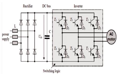
In general, two basic types of inverters exist: Voltage Source Inverter (VSI), employing a dc link capacitor and providing a switched voltage waveform, and Current Source Inverter (CSI), employing a dc link inductance and providing a switched current waveform at the motor terminals [1]. Figure 1 shows a basic three-phase voltage source converter circuit. CS inverters are robust in operation and reliable due to the insensitivity to short circuits and noisy environment. VS inverters are more common compared to CS inverter since the use of Pulse Width Modulation (PWM) allows efficient and smooth operation, free from torque pulsations and cogging [Bose 97]. Furthermore, the frequency range of VSI is higher and they are usually more inexpensive when compared to CSI drives of the same rating [Dub 89]. Here, only voltagesource inverters are considered. Although the power flow through the device is reversible, it is called an inverter because the predominant power flow is from the dc bus to the three-phase ac motor load. Bi-directional power flow is an important feature for motor drives as it allows regenerative breaking, i.e., the kinetic energy of the motor and its load is recovered and returned to the grid when the motor slows down [2]. In electric vehicle application, the dc bus energy is supplied directly from primary energy sources (e.g., Batteries).
Figure 1. Basic Three-Phase Voltage-Source Converter Circuit
Figure 2 presents typical voltage and current waveforms of a B6-diode bridge supplied by a stiff grid. As indicated by the dashed lines, the rectifier current iB6 increases, if the absolute value of a line voltage is higher than the dc voltage. Consequently, the dc voltage increases slightly. A dc voltage higher than the current voltage supply causes a reduction of the rectifier input current until the current equals zero and the diode bridge blocks the supply voltage. The rectifier current iB6 is identically reflected by the line currents. The sign of each line current depends on the two non-blocking diodes each conducting the positive and negative rectifier current, respectively. During the conducting period, the difference of line and dc voltage is active as voltage drop over the line inductances and resistances [3]. The higher the line inductances, the smaller the line current peaks. However, the value of the line inductances is limited due to economic and efficiency reasons. Furthermore, the average dc voltage depends on the line inductances and the inverter output power. The maximum dc voltage (no load) is equal to the maximum amplitude of the line voltages. Due to voltage drops of line inductances, resistances and rectifier diodes, the dc voltage slightly decreases with increasing load [4]. According to Figure 1, the dc voltage is switched in a three-phase PWM inverter by six semiconductor switches in order to obtain pulses, forming three-phase ac voltage with the required frequency and amplitude for motor supply. The switching devices must be capable of being turned “on” as well as turned “off”. During the last years, major progress has been made in the development of new power semiconductor devices. The simpler requirement driving the power switches and the higher maximum switchingfrequency, enabling higher operating frequencies (higher motor speed), provide continually rising output power. The new generation of switching devices is capable of conducting more current and blocking higher voltages. The alternatives at present are Gate Turn-off thyristor (GTO), MOS Controlled Thyristor (MCT), Bipolar Junction Transistor (BJT), MOS Field Effect Transistor (MOSFET) and Insulated Gate Bipolar Transistor (IGBT) [7]. The IGBT is a combination of power MOSFET and bipolar transistor technology and combines the advantages of both. In the same way as a MOSFET, the gate of the IGBT is isolated and its driving power is very low. However, the conducting voltage is similar to that of a bipolar transistor. Presently, IGBTs dominate the medium-power range of variable speed drives. Since the maximal current rating of IGBT modules is around 1 kA and the voltage rating is approximately 3 kV, they will gradually replace GTOs at higher power levels [Vas 99] [8]. Parallel to the power switches, reverse recovery diodes are placed conducting the current depending on the switching states and current sign. These diodes are required, since switching off an inductive load current generates high voltage peaks probably destroying the power switch.
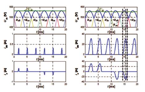
Figure 2. Typical Voltage and Current Waveforms of a B6-Diode
Exemplary for one inverter leg, Figure 3 presents the basic configuration and the inverter output voltage depending on the switching state and current sign. The basic configuration of one inverter output phase consists of upper and lower power devices T1 and T4, and reverses recovery diodes D1 and D4. When transistor T1 is on, a voltage ½ is Vdc applied to the load. With the development of the technique of Pulse Width Modulation (PWM), the control technique of four-quadrant operated inverters, the field-orientated control of synchronous machines and induction machines in low and middle power level on the one side and the rapid development of semiconductor devices, for example the appearing of GTO, IGBT and IGCT in Mega Watt power level on the other side, nowadays the application range of technology of power electronics is growing in the field of electrical drives, power propulsion systems for ships and utility apparatus in power systems towards the Multi-Mega watt power level, for example, with Flexible Alternating Current Transmission Systems (FACTS) devices [13]. Besides the two-level converter, the three-level converter has been used for high power applications for a reasonable modulation performance; furthermore it has more attractive technical advantages for the application in the high power level from today's view [1]. Different PWM techniques are Single Pulse Modulation, Multiple Pulse Modulation and Sinusoidal Pulse Modulation.
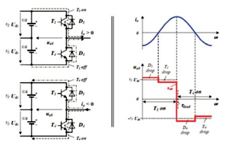
Figure 3. Basic Configuration of a Half - Bridge Inverter and Centre Tap Inverter Output Voltage
The output voltage from single-phase full-bridge inverter and the block diagram are shown in Figure 4 and Figure 5. The harmonic content can be reduced by using several pulses in each half-cycle of output voltage [10]. The generation of gating signals for turning on and off transistors is shown in Figure 4. The gating signals are produced by comparing reference signal with triangular carrier wave. The frequency of the reference signal sets the output frequency (fo) and carrier frequency (fc) determine the number of pulses per half cycle, p. The variation of modulation index (M) from 0 to 1 varies the pulse from 0 to π/p and the output voltage from 0 to Vm as given in Figure 6.
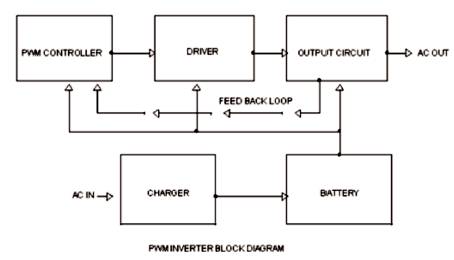
Figure 4. Block Diagram of PWM Inverter
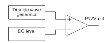
Figure 5. Block Diagram of Single Pulse Modulation
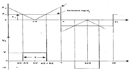
Figure 6. Waveform of Single Pulse Modulation
Three-phase reference voltages of variable amplitude and frequency are compared in three separate comparators with a common triangular carrier wave of fixed amplitude and frequency (Figure 4 & Figure 5). Each comparator output forms the switching-state of the corresponding inverter leg [Dub 89], [Leo 85]. In torque controlled ac motor drives using sinusoidal PWM, the reference voltages (u*a, u* b,u*c ) are usually calculated by an additional current control loop (FOC).
As shown in Figure 7, a saw-tooth or triangular-shaped carrier wave, determining the fixed PWM frequency, is simultaneously used for all three phases. This modulation technique, also known as PWM with natural sampling, is called sinusoidal PWM because the pulse width is a sinusoidal function of the angular position in the reference signal [15]. Since the PWM frequency, equal to the frequency of the carrier wave, is usually much higher than the frequency of the reference voltage, the reference voltage is nearly constant during one PWM period TPWM. This approximation is especially true considering the sampled data structure within a digital control system. Depending on the switching states, the positive or negative half dc bus voltage is applied to each phase. At the modulation stage, the reference voltage is multiplied by the inverse half dc bus voltage compensating the final inverter amplification [6].
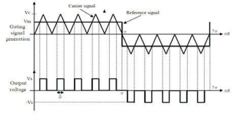
Figure 7. Multi- Pulse Width Modulation
Numerous industrial applications have begun to require higher power apparatus in recent years. Some medium voltage motor drives and utility applications require medium voltage and megawatt power level. For a medium voltage grid, it is troublesome to connect only one power semiconductor switch directly. As a result, a multilevel power converter structure has been introduced as an alternative in high power and medium voltage situations [5]. A multilevel converter not only achieves high power ratings, but also enables the use of renewable energy sources. Renewable energy sources such as photovoltaic, wind, and fuel cells can be easily interfaced to a multilevel converter system for a high power application.
In Figure 8, each of the three phases of the inverter shares a common bus, which has been subdivided by five capacitors into six levels. The voltage across each capacitor is Vdc, and the voltage stress across each switching device is limited to Vdc through the clamping diodes. Table 1 lists the output voltage levels possible for one phase of the inverter with the negative dc rail voltage V0 as a reference. State condition 1 means the switch is on, and 0 means the switch is off.
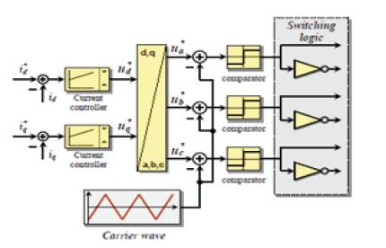
Figure 8. Sinusoidal PWM, Current Control and Switching Logic
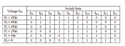
Table1. Switching States of Diodes
Each phase has five complementary switch pairs such that turning on one of the switches of the pair require that the other complementary switch be turned off. The complementary switch pairs for phase lag are (Sa1, Sa'1), (Sa2, Sa'2), (Sa3, Sa'3), (Sa4, Sa'4), and (Sa5, Sa'5 ). Table 1 also shows that in a diode-clamped inverter, the switches that are on for a particular phase leg is always adjacent and in series. For a six-level inverter, a set of five switches is on at any given time. The line voltage Vab consists of a phase-leg a voltage and a phase-leg b voltage. The resulting line voltage is an 11-level staircase waveform. This means that an m-level diode-clamped inverter has an m-level output phase voltage and a (2m-1) level output line voltage. Although each active switching device is required to block only a voltage level of Vdc, the clamping diodes require different ratings for reverse voltage blocking. Using phase a of Figure 9 as an example, when all the lower switches Sa'1 through Sa'5 are turned on, D4 must block four voltage levels, or 4Vdc . Similarly, D3 must block 3Vdc , D2 must block 2Vdc , and D1 must block Vdc . If the inverter is designed such that each blocking diode has the same voltage rating as the active switches, Dn will require n diodes in series; consequently, the number of diodes required for each phase would be (m-1) × (m-2). Thus, the number of blocking diodes is quadratically related to the number of levels in a diode-clamped converter. One application of the multilevel diode-clamped inverter is an interface between a high-voltage dc transmission line and an ac transmission line. Another application would be as a variable speed drive for high-power medium-voltage (2.4 kV to 13.8 kV) motors as proposed in Static var compensation is an additional function for which several authors have proposed for the diode-clamped converter [9].
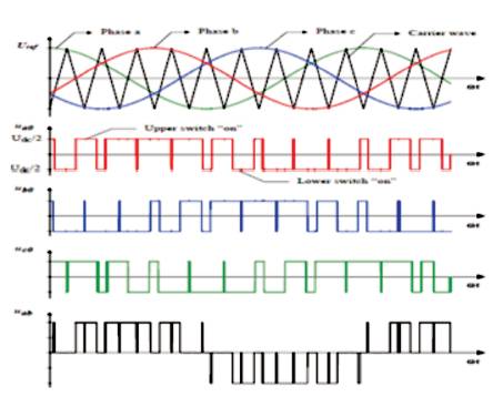
Figure 9. Principle of Sinusoidal PWM Generation
Meynard and Foch introduced a flying-capacitor-based inverter in 1992. The structure of this inverter is similar to that of the diode-clamped inverter except that instead of using clamping diodes, the inverter uses capacitors in their place. The circuit topology of the flying capacitor multilevel inverter is shown in Figure 10. This topology has a ladder structure of dc side capacitors, where the voltage on each capacitor differs from that of the next capacitor. The voltage increment between two adjacent capacitor legs gives the size of the voltage steps in the output waveform [16] [12].
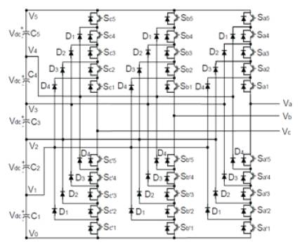
Figure 10. Three-Phase Six-Level Structure of a Diode-Clamped inverter
Cascade Multilevel Inverter (CMLI) is one of the most important topology in the family of multilevel and multi pulse inverters. It requires least number of components when compared to diode-clamped and flying capacitors type multilevel inverters and no specially designed transformer is needed as compared to multipulse inverter. It has modular structure with simple switching strategy and occupies less space [5] [6] .
The CMLI consists of a number of H-bridge inverter units with separate dc source for each unit and is connected in cascade or series as shown in Figure 10. Each H-bridge can produce three different voltage levels: +Vdc , 0, and –Vdc by connecting the dc source to ac output side by different combinations of the four switches S1 , S2 , S3 , and S4 as in table 1. The ac output of each H-bridge is connected in series such that the synthesized output voltage waveform is the sum of all of the individual H-bridge outputs [4].
By connecting the sufficient number of H-bridges in cascade and using proper modulation scheme, a nearly sinusoidal output voltage waveform can be synthesized. The number of levels in the output phase voltage is 2s+1, where s is the number of H-bridges used per phase. Figure 11 shows a 6-level output phase voltage waveform using three H-bridges. The magnitude of the ac output phase voltage is given by Van = Va1 + Va2+ Va3 [7][4]. The main features of a Cascaded H-Bridge with source inverters have been used.
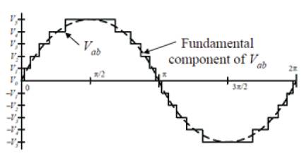
Figure 11. Line Voltage Waveform for a Six Level Diode Clamped Inverter.
From Figure 11, the magnitudes of the Fourier coefficients when normalized with respect to Vdc are derived as follows:
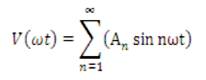
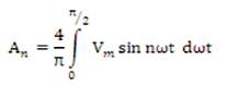
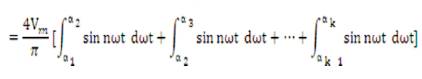
Further simplification of the equation (2) and substituting them in equation (1) gives the voltage equation for Van
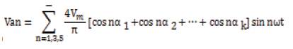
The conducting angles, α0, α 1... αk , can be chosen such that the voltage total harmonic distortion is a minimum. Generally, these angles are chosen so that predominant lower frequency harmonics, 3rd , 5th , 7th , 11th , and 13th harmonics are eliminated.
For a 7-level cascade inverter, there are three H-bridges per phase i.e., s = 3 or three degrees of freedom are available and is shown in Table 2. One degree of freedom is used to control the magnitude of the fundamental voltage and the remaining two degrees of freedom are used to eliminate 5th , 7th , 11th , and 13th order harmonic components as they dominate the total harmonic distortion [4] [15].
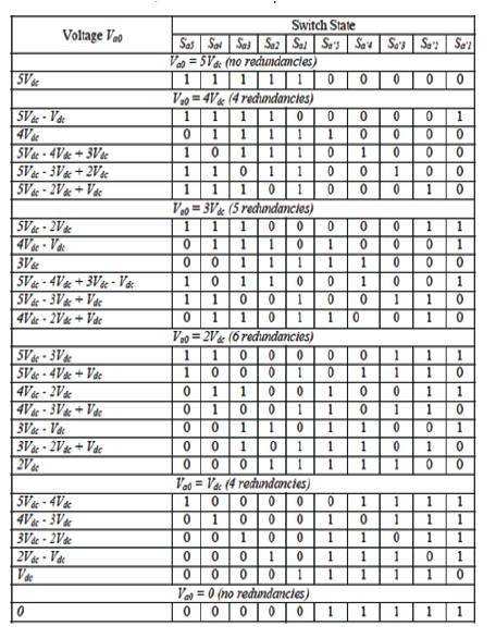
Table 2. Flying - Capacitor Six - Level Inverter with Redundant Voltage Levels and Corresponding Switch States.
Multilevel cascaded inverters have been proposed for such applications as static var generation, an interface with renewable energy sources, and for battery-based applications. Three-phase cascaded inverters can be connected in wyes, or in delta. Peng has demonstrated a prototype multilevel cascaded static variable generator connected in parallel with the electrical system that could supply or draw reactive current from an electrical system. The inverter could be controlled to either regulate the power factor of the current drawn from the source or the bus voltage of the electrical system where the inverter was connected. Peng and Joos have also shown that a cascade inverter can be directly connected in series with the electrical system for static var compensation as in Figure 12. Cascaded inverters are ideal for connecting renewable energy sources with an ac grid, because of the need for separate dc sources, which is the case in applications such as photovoltaics or fuel cells [17] [18].
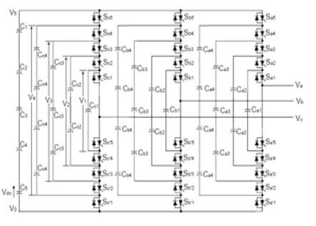
Figure 12. Three - Phase Six - Level Structure of a Flying Capacitor Inverter.
Cascaded inverters have also been proposed to use as the main traction drive in electric vehicles, where several batteries or ultra capacitors are well suited to serve as SDCSs. The cascaded inverter could also serve as a rectifier/charger for the batteries of an electric vehicle while the vehicle was connected to an ac supply [14] .
A Genetic Algorithm (GA) is a programming technique that mimics biological evolution as a problem-solving strategy. Given a specific problem to solve, the input to the GA is a set of potential solutions to that problem, encoded in some fashion, and a metric called a fitness function that allows each candidate to be quantitatively evaluated. The GA then evaluates each candidate according to the fitness function. In a pool of randomly generated candidates, of course, most will not work at all, and these will be deleted. However, purely by chance, a few may hold promise - they may show activity, even if only weak and imperfect activity, toward solving the problem.
Before a genetic algorithm can be put to work on any problem, a method is needed to encode potential solutions to that problem in a form that a computer can process. One common approach is to encode solutions as binary strings: sequences of 1's and 0's, where the digit at each position represents the value of some aspect of the solution. Another, similar approach is to encode solutions as arrays of integers or decimal numbers, with each position again representing some particular aspect of the solution. This approach allows for greater precision and complexity than the comparatively restricted method of using binary numbers only and often "is intuitively closer to the problem space”.
These promising candidates are kept and allowed to reproduce. Multiple copies are made of them, but the copies are not perfect; random changes are introduced during the copying process. These digital offspring then go on to the next generation, forming a new pool of candidate solutions, and are subjected to a second round of fitness evaluation. Those candidate solutions which were worsened, or made no better, by the changes to their code are again deleted; but again, purely by chance, the random variations introduced into the population may have improved some individuals, making them into better, more complete or more efficient solutions to the problem at hand [11]. Again these winning individuals are selected and copied over into the next generation with random changes, and the process repeats. The expectation is that the average fitness of the population will increase each round, and so by repeating this process for hundreds or thousands of rounds, very good solutions to the problem can be discovered. As astonishing and counterintuitive as it may seem to some, genetic algorithms have proven to be an enormously powerful and successful problem-solving strategy, dramatically demonstrating the power of evolutionary principles. Genetic algorithms have been used in a wide variety of fields to evolve solution to the problems as difficult as or more difficult than those faced by human designers. Moreover, the solutions they come up with are often more efficient, more elegant, or more complex than anything comparable a human engineer would produce. In some cases, genetic algorithms have come up with solutions that baffle the programmers who wrote the algorithms in the first place.
There are many different techniques which a genetic algorithm can use to select the individuals to be copied over into the next generation, but listed here are some of the most common methods. Some of these methods are mutually exclusive, but others can be and often are used in combination. The different selection techniques are elitist selection, fitness-proportionate selection, roulettewheel selection, scaling selection, tournament selection, rank selection, generational selection, steady-state selection, hierarchical selection. These selection techniques are the mostly used ones in the present day and in many ways helps in solving several problems in genetic algorithm.
The flowchart shown in Figure 13 gives the procedure for the execution of the Genetic Algorithm method. Initially, the control variables are identified and the parameters are decided to generate the initial population. Once this is done, the fitness of each chromosome within the initial population is evaluated. Then the selection process for the methods, either mutation or crossover, is done and finally the healthy population is obtained. The paper deals with hardware circuit diagram of the selective harmonic elimination of multi level inverter using genetic algorithm as in Figure 14. It consists of power supply, driver circuit, controller unit and the main circuit. The available AC voltage of 230V is given to the primary side of the transformer from a source. The voltage at the primary side is step-down to 12V at the secondary side by a transformer and given to the driver circuit. The driver circuits, which are controlled by micro controller, consist of opto-coupler.
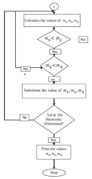
Figure 13. Procedure for the Execution of the Genetic Algorithm
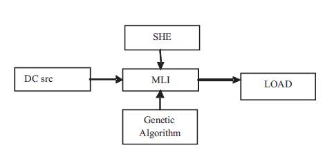
Figure 14. Block Diagram of the Genetic Algorithm
Here we can use the electrolytic capacitor. This eliminates the harmonics from both voltage and current signals. This 12V is converted to DC and regulated by means of regulator 7805. After passing through regulator, the voltage maintains a constant value. On comparing Figures 16 and 17, a model is simulated using Matlab as shown in Figure 15.
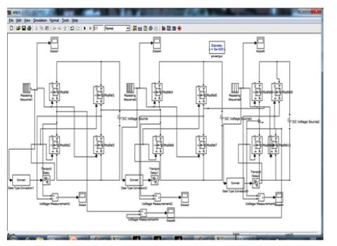
Figure 15. Matlab Simulation
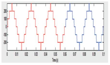
Figure 16. Simulation Output Before Applying Genetic Algorithm
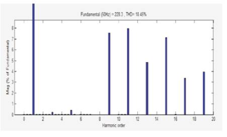
Figure 17. Fast Fourier Transform.
The input voltage is 12V AC which is obraived from step down transformer. This AC supply is converted to a DC voltage by using a diode bridge rectifier. The pin assignments for DIP in Figure 18 and the schematic diagram of the circuit has been given in Figure 19. Output from the rectifier unit having harmonic contents, so the author provided the filter circuit, filter circuit is used to reduce the harmonics. Filter circuit makes it possible for the elimination of unwanted harmonics or signal and make the system distortion free. A distortion free circuit is reliable, accurate and always clear.
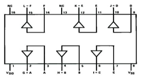
Figure 18. Pin Assignments for DIP
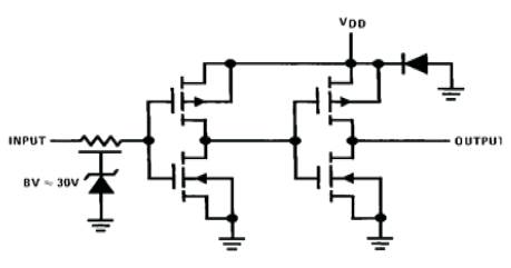
Figure 19. Schematic Diagram
Basically, the simplest way to visualize an opto-coupler is in terms of its two main components: the input LED and the output transistor or diac. As the two are electrically isolated, this gives a fair amount of flexibility when it comes to connecting them into circuit. All we really have to do is work out a convenient way of turning the input LED on and off, and using the resulting switching of the phototransistor/ diac to generate an output waveform or logic signal that is compatible with our output circuitry. This circuit consists of a bridge rectifier, and filter. Table 3 and 4 gives the maximum ratings and operating conditions. Voltage regulator and PIC microcontroller. Microcontroller is the main part of the hardware design. The supply is stepped down and given to the controller unit. A suitable program is fed to the controller circuit to generate the required pulses. The control circuit uses PIC microcontroller. The pin diagram has been given in Figure 20. The driving pulses required for the MOSFET is obtained from this circuit.
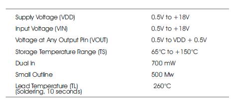
Table.3 Absolute Maximum Ratings
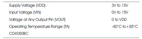
Table.4 Recommended Operating Conditions
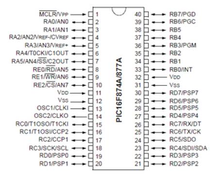
Figure 20. Pin Diagram
Rectifier circuit, which converts ac voltage into pulsating dc voltage. In this, diagonally opposite pair of diodes are made to conduct by giving ac supply. The bridge rectifier converts the given ac voltage to dc voltage. A rectifier is a device which offers a low resistance to the current in one direction and a high resistance in the opposite direction. Such a device is capable of converting A.C. voltage into a pulsating D.C. voltage. The rectifier employs one or more diodes. It may be either a vacuum diode or a semiconductor diode. Bridge rectifier is a full wave rectifier. It consists of four diodes, arranged in the form of a bridge. It utilizes the advantages of the full wave rectifier and at the same time, it eliminates the need for a centre tapped transformer. The supply input and the rectified output are the two diagonally opposite terminals of the bridge. During the positive half cycle, the secondary terminal A is positive with respect to terminal B. Now the diodes D1 and D3 are forward biased and hence do not conduct. The current flows from terminal A to terminal B through D1, load resistance RL and the diode D3 and then through the secondary of the transformer. During the negative half cycle, terminal B is positive with respect to point A. Now diodes D2 and D4 are forward biased and hence conduct. Diode D1 and D3 are reverse biased and hence do not conduct. The current flows from terminal B to terminal A through diode D2, the load resistance RL and diode D4 and then through the secondary of the transformer. On both positive and negative half cycles of the A.C. input, the current flows through the load resistance RL in the same direction. The polarity of the voltage developed across RL is such that, the end connected to the junction of the diodes D1 and D2 will be positive.
The function of the circuit element is to remove the fluctuation / pulsation (called as ripple) present in the output voltage supplied by the rectifier. It cannot give a ripple free voltage as that of dc battery, but it approaches so closely that, the power supply performs so well. Output from the rectifier unit having harmonic contents, so the filter circuit, is used to reduce the harmonics. The electrolytic capacitor is used to eliminate the harmonics from both voltage and current signals. Voltage regulator is used to maintain the constant voltage with the variation of the supply voltage and the load current. When specifying individual ICs within this family, the xx is replaced with a two-digit number, which indicates the output voltage, the particular device is designed to provide (for example, the 7805 has a 5 volt output, while the 7812 produces 12 volts). The 78xx lines are positive voltage regulators, meaning that they are designed to produce a voltage that is positive relative to a common ground. The MOSFET is used for switching in the inverter circuit. This N-Channel enhancement mode silicon gate power field effect transistor is an advanced power MOSFET designed, tested, and guaranteed to withstand a specified level of energy in the breakdown avalanche mode of operation. All of these power MOSFETs are designed for applications such as switching regulators, switching converters, motor drivers, relay drivers, and drivers for high power bipolar switching transistors requiring high speed and low gate drive power. These types can be operated directly from integrated circuits.
The hardware model of selective harmonic elimination of harmonics using genetic algorithm yields the output shown in Figure 21. The output obtained is of stepped nature with seven levels. The THD and harmonics gets reduced in this waveform.
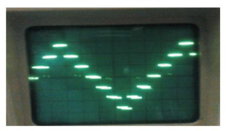
Figure 21. Output Waveform of Hardware Model
The literature survey is done using the materials that were obtained through different sources. In this project, the author analyzed the principles of Pulse Width Modulation technique and different methods that are involved are studied in detail. Finally, we opt Sinusoidal Pulse Modulation technique to be the best method of producing a trigger pulse with lower order harmonics getting reduced to a considerable level. Next the primary thing that have to be considered is the type of multi level inverter configuration. The different type of Multi Level Inverters is also investigated. Their advantages and disadvantages are studied in detail. The best type being advantageous over other methods is Cascaded H- Bridge separate source inverter, hence it is selected. The simulation is done and the output waveforms of multilevel inverters are in a stepped form, therefore they have reduced harmonics compared to a square wave inverter. But the results are found to have odd harmonics and Total Harmonic Distortion (THD).
Several methods with their advantages and disadvantages are collected from the previous papers and a survey is done. At the end of the survey, we selected Genetic Algorithm Technique to reduce the odd harmonics by finding the exact triggering pulse. The main reason for selecting this method is that, it solves the problem with a simpler formulation and with any number of levels without extensive derivation of analytical expressions. When the pulses, generated, are given to the circuit the odd harmonics gets reduced to a significant level. Thus, a survey over the harmonic elimination in Multi Level Inverters is done and successfully arrived at a solution as per the objective. This paper recommends the use of improvised model of multilevel inverters in electronics industry and various power systems.
iB6 – Rectifier current
T1 – First transistor
T4 – Fourth transistor
D1– First diode
D2 – Second diode
D3 – Third diode
D4 – Fourth diode
Vdc– DC Voltage
Ua– Reference voltage
Ub– Reference voltage
Uc– Reference voltage
Dn – nth diode
n – Number of diodes
m – Number of level output phases
s – Number of H-bridges used per phase
S – Switches
Van – Output phase voltage
t - Time constant
T – Time interval
ω – Angular frequency
An– Output phases
Vm– Maximum voltage
αk – Conducting angles
TS – Storage Temperature Range
VDD – Supply Voltage
VIN – Input Voltage
TL– Lead Temperature
VOUT – Voltage at any Output Pin
TA – Operating Temperature Range
DIP – Dual In Package