(1)
Analog integrated circuit design is receiving a tremendous boost due to the development and application of Current- Mode (CM) processing. Application of CM techniques provides wider bandwidth; which is virtually independent of the closed loop gain, greater linearity and large dynamic range. The Operational Transresistance Amplifier (OTRA) has emerged as an effective alternate current mode analog building block. It is a high gain current input, voltage output amplifier and also free from parasitic input capacitances and resistances as its input terminals are virtually grounded thus eliminating response limitations due to parasitics. OTRA is used as an analog building block for realizing a number of circuits having applications in signal processing and generation. Precise rectification is an important requirement in instrumentation and measurement circuits and is addressed in this paper. Traditionally, diodes are used to build rectifiers however; rectification is not permitted below a voltage of ∼ 0.7 V for silicon and ∼ 0.3 V for germanium diodes due to cutin voltage. For low voltage applications, Operational Amplifiers (OPAMP) with diode connected in feedback is used which prevents the fast switching of the diodes in high frequency range due to slew rate limitation of OPAMP. This paper aims at presenting an OTRA based FWR which is suitable for low voltage rectification. The functionality of the proposed circuit is validated through SPICE simulation for which OTRA is realized using Current Feedback Operational Amplifier (CFOA).The simulation results are found in close agreement to the theoretical results.
State-of-the-Art analog integrated circuit design is receiving a tremendous boost due to the development and application of current-mode processing (Yuan, 2007). .It is well known that, the key performance features of current-mode technique are inherent wide bandwidth; which is virtually independent of closed loop gain, greater linearity and large dynamic range. Recently Operational Transresistance Amplifier (OTRA) has emerged as an effective alternate analog building block. It is a high gain current input, voltage output amplifier (Salama & Soliman, 1999). OTRA being a current processing building block, inherits all the advantages of current mode technique. It is also free from parasitic input capacitances and resistances as its input terminals are virtually grounded thus eliminating response limitations due to parasitics. OTRA is now being used as an analog building block for realizing a number of circuits having applications in signal processing and generation (Salama & Soliman, (1999), Cam, (2002), Pandey, Pandey, Paul, Singh, Sriram, and Trivedi, (2014), Bothra, Pandey, Pandey & Paul, (2013)).
Precise rectification is one of the important requirements in instrumentation and measurement. It finds application in ac voltmeters, signal-polarity detectors, averaging circuits, sample-and-hold circuits, peak value detectors and amplitude-modulated signal detectors (Gayakwad, (2007), Gift, (2000), Gift & Maundy, (2007)). In general, diodes are used as rectifiers however; rectification is not permitted below a voltage of ∼0.7 V for silicon and ∼0.3 V for germanium diodes due to threshold voltage. Lowvoltage rectification is required in applications such as amplitude modulated signal detectors. Conventionally, low-voltage full wave rectification is obtained using Operational Amplifiers (OPAMP) with diode connected in feedback (Gift, (2000), Gift & Maundy, (2007)). However, slew rate limitation of OPAMP prevents the fast switching of the diodes in high frequency range and hence results in distortion. A variety of precision FWRs using various current mode building blocks such as Current Conveyor (CC) and its variants(C. Toumazou, Lidgey & Chattong, (1994) , Hayatleh, Porta & Lidgey (1995) , Monpapassorn, Dejhan & Cheevasuvit, (2001) , Surakumpontorn, Anuntahirunrat & Riewruja,(1998), Yuce, Minaei & Cicekoglu, (2006) , Kumngern, 2011)) , Operational Transconductance Amplifier (OTA) (Jongkunstidchai, Fongsamut, Kumwachara, Surakampontorn, 2007) , Current Follower (CF) (Tiliute , 2003) and (Biolek, Hancioglu, Keskin, 2008) CDTA (Koton, Herencsar, Vrba, Minaei (2011) , Khateb, Vávra & Biolek, (2010) , Tangsrirat, Pukkalanun & Surakampontorn, (2011)) have been reported in literature. The circuits proposed in(Toumazou, Lidgey & Chattong, 1994) , Hayatleh, Porta & Lidgey, (1995)) make use of diodes whereas the circuit of (Monpapassorn, Dejhan & Cheevasuvit, 2001) employs bipolar current mirrors in addition to CCII. The FWR circuits of (Surakumpontorn, Anuntahirunrat & Riewruja, (1998) , Jongkunstidchai, Fongsamut, Kumwachara, Surakampontorn, (2007)) employ excessive number of active blocks. Circuit proposed in (Yuce, Minaei & Cicekoglu, 2006) employs two CCII and two MOS transistors and that presented in(Kumngern, 2011) employs two Differential Difference Current Conveyor (DDCC). The circuits of (Tiliute, (2003), Biolek, Hancioglu, Keskin, (2008) , Koton, Herencsar, Vrba, Minaei (2011) , , Khateb, Vávra & Biolek, (2010) Tangsrirat, Pukkalanun & Surakampontorn, (2011)) provide current outputs which need to be converted back to voltage for circuits requiring voltage inputs, which would considerably increase the component count.
This paper presents OTRA based FWR which is suitable for low voltage rectification. Active only implementation of the proposed circuit is also presented wherein the passive resistors connected to input terminals of OTRA have been implemented using MOS transistors operating in linear region (Salama & Soliman, 1999). The performance of the proposed FWR has been verified through SPICE simulation.
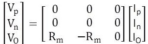
OTRA is a high gain current input voltage output device. The input terminals of OTRA are internally grounded, thereby eliminating response limitations due to parasitic capacitances and resistances and hence is appropriate for high frequency operation. The circuit symbol of OTRA is shown in Figure 1 and the port characteristics are given by equation (1), where Rm is the transresistance gain of OTRA. For ideal operations the Rm of OTRA approaches infinity and forces the input currents to be equal. Thus OTRA must be used in a negative feedback configuration.
The proposed FWR is shown in Figure 2. The circuitry comprising of OTRA1, two resistances of value R1 each is a simple inverter, while OTRA2 is used in open loop configuration to work as comparator.
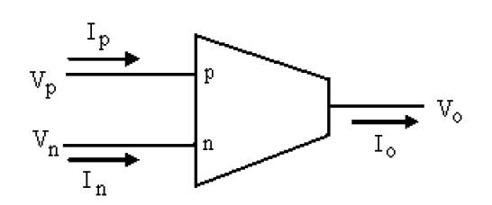
Figure 1. OTRA Circuit Symbol.
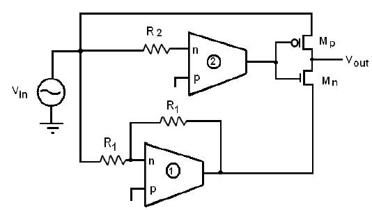
Figure 2. OTRA Based Proposed FWR.
Considering a sinusoidal signal to be applied at comparator input is represented as,
The current In through n terminal of OTRA2 is given by
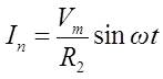
The p terminal current (Ip ) for OTRA 2 being zero, the output of the comparator will be at positive saturation level +Vsat for negative half cycle of vin and at –Vsat during positive halfcycle. Thus comparator provides a periodic rectangular output which drives the gates of two MOS switches (Mp and Mn ) with their sources connected to +Vin and –Vin respectively. For positive half cycle of the input, a negative voltage is developed at the output of comparator which in turn makes the transistor Mp ON while Mn remains OFF. This makes the output voltage Vout to follow the input signal for positive half cycle. During negative half cycle of the input, the transistor Mn turns ON and Mp goes OFF producing an output in phase opposition with input signal thus making unidirectional output.
The current differencing property of the OTRA makes it possible to implement the resistors connected to the input terminals of OTRA, using MOS transistors with complete non-linearity cancellation, (Salama & Soliman, 1999). Each resistor requires two matched n-MOSFETs connected in a manner is shown in Figure 3.
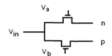
Figure 3.MOS Based Resistor
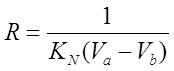
Symbols '+' and '-' represent the non-inverting and the inverting terminals of the OTRA. The voltages at the drain and the source terminals for both MOSFETs are equal. On taking the difference of the currents flowing in the two transistors, the non linearity gets cancelled out. The following equation defines the resistor that has been realized.
where,
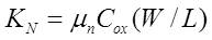
and μ, Cox and W/L represent standard transistor parameters.
The KN needs to be determined for the transistors being used to implement the resistors. The choice of voltages Va and Vb is important. The circuit shown in Figure 3, realizes a resistor of value expressed by equation (4) at the inverting terminal. If it is desired to realize a resistor of the same value at the non-inverting terminal, then Va and Vb must be interchanged. The MOS realization of circuit of Figure 2, is shown in Figure 4.
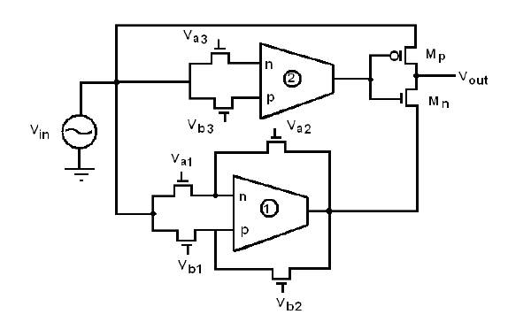
Figure 4. MOS Based Realization of Proposed FWR
For this application, the OTRA was realized using AD844 CFOA IC is shown in Figure 5 (Hou, Chien & Lo, 2005). The equivalent circuit of Figure 5 for non ideal analysis (Lo, Chien & Chiu, 2008) is presented in Figure 6. The CFOAs have been replaced with current conveyors having finite input resistances (RX) and finite resistance at its Z terminal (RZ). Ideally the input resistance at the X terminal is zero and is infinite at the Z terminal. For the AD844 CFOA, the input resistance RX is around 50 Ω and RZ is around 3 MΩ (AD844).
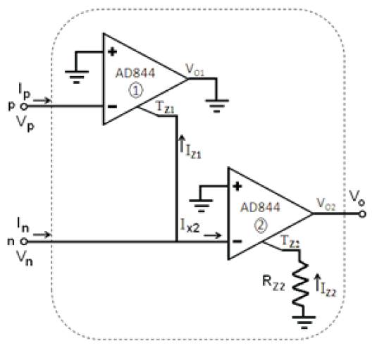
Figure 5. OTRA Constructed with AD844
From Figure 6, various currents, assuming RX1 = RX2 = R X and RZ1 = RZ2 = RZ, can be calculated as follows:


Ideally ID should be equal to IZ1 , which can be approximated only if RZ >>RX , which is true for AD844. Also the approximation that the input terminals are virtually grounded will be true only if the external resistance at the input terminal of the OTRA is much larger than RX. If these two conditions are satisfied, the OTRA constructed with AD844 closely approximates an ideal OTRA. From equation (6)-(9) the output voltage VO, taking into account the above mentioned approximations, can be calculated as:
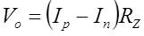
Where, RZ is the transresistance of the OTRA.
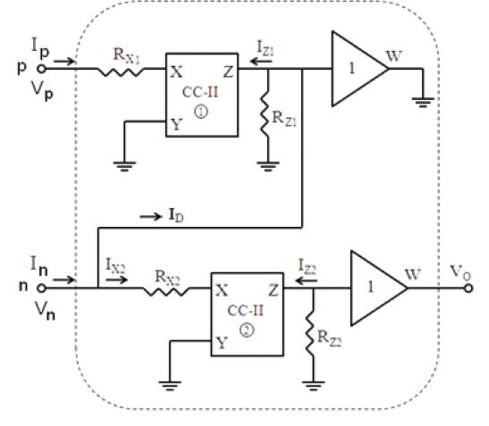
Figure 6. Equivalent Circuit of OTRA Constructed with AD844
The proposed theoretical predictions are validated through simulations using PSPICE macro model of CFOA AD844 IC is shown in Figure 7. Supply voltages used are ±15 V. The circuit of Figure 2 is excited by a 100 mV,100 KHz sinusoidal input signal, resulting in a rectangular waveform at the output of comparator saturating at ±10 V.
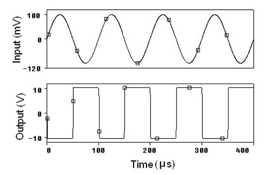
Figure 7. Output of Comparator for a 100 mV, 100 KHz Input Excitation.
The time domain response of the proposed circuit for 200 mV, 50 Hz sinusoidal excitation is shown in Figure 8 (a) and its frequency spectrum is depicted in Figure 8 (b). Similarly the transient response for 200 mV, 50 KHz is given in Figure 9 (a) whereas Figure 9 (b) represents the frequency spectrum. The simulated ripple factor for the proposed circuit for different input frequencies is observed and the worst case value observed is 0.52.
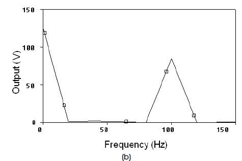
Figure 8. Output of the Proposed Circuit for 200 mV, 50Hz Input Signal (a) Time Domain (b) Frequency Spectrum
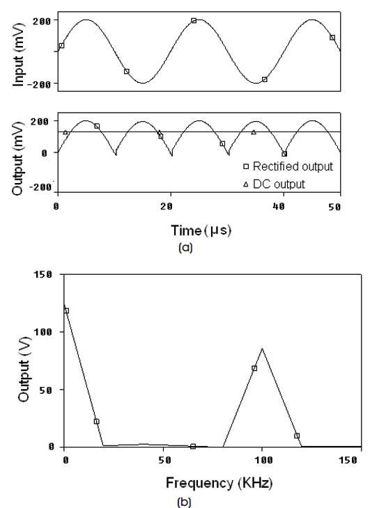
Figure 9. Output of the Proposed Circuit for 200 mV, 50KHz Input Signal (a) Time Domain (b) Frequency Spectrum
The DC transfer characteristics of the proposed circuit is also studied and shown in Figure 10. It may be noted that behavior of the proposed circuit is linear for an input voltage range between -10 V to +10 V.
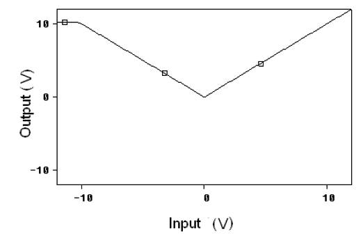
Figure 10. DC Response of the Proposed Circuit
Precise rectification is an important requirement in instrumentation and measurement circuits. Rectifiers are traditionally designed using diodes, but due to cut-in voltage limitation, these circuits cannot be used for rectification of voltages below 0.7 V /0.3 V for silicon/ germanium diodes respectively. For low voltage rectification, OPAMP based circuits with diode connected in feedback are used. However, due to slew rate limitation of OPAMP fast switching of the diodes in high frequency range is not possible.
This paper presents a precision full-wave rectifier using OTRA which has emerged relatively recently as an effective current mode analog building block. It is a high gain current input, voltage output amplifier and is not slew limited in the same manner as voltage mode OPAMP. The proposed circuit makes use of two OTRAs and two MOS switches. The circuit is suitable for low voltage rectification and provides output voltage amplitude almost equal to input voltage as there is no threshold voltage constraint. The theoretical proposition is verified through SPICE simulation using CFOA based OTRA realization. The simulation results are observed to be in close agreement to the theoretical results.