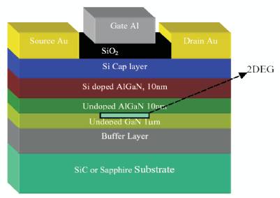
Figure 1. Structure of AlGaN/GaN HEMT [1]
In this paper, parametric influence on noise in HEMT LNA designed using FR4 substrate was analyzed. At higher frequencies of operation high electron mobility transistor designs are often influenced by shot noise and this shot noise is depended on different parameters of the device. This design is carried out at a centre frequency of 5.8GHz and critical parameters like gate resistance, transconductance; gate source biasing values influence on noise immunity of this design is analyzed in the frequency range of 1GHz to 10GHz. Variation of Maximum Gain and Noise Figure w.r.t to frequency were obtained for different parametric values. Obtained results had given better understanding of the noise influence on the design performance under different constraints pertained to parameter variation. These observations are in greater agreement with the theoretical facts. This work is carried out using ADS simulation software.
Recent developments in the field of IC technology have forced the researchers across the globe to ensure the progress of the technology get undamped with ever increasing demands. In this attempt, naturally developments in the field of microelectronics are seen. Earlier works in this field are pertained to use of different combinations of semiconductor materials as substrates and the studies related to the characterization of the high speed and high performance devices like HEMTs. In the later stages, the focus shifted towards enhancing the performance of these devices for various applications. Equivalent circuits were developed to characterize and study the electrical nature of these devices. [1] An equivalent circuit can consists of extrinsic and intrinsic parts, which commonly represent these HEMTs. The intrinsic part described in terms of state functions, whereas the extrinsic component describes the device layout. [1, 7 and 8] Later, device simulations were done to ensure the credibility of this device performance at different frequency ranges. These devices are in general fabricated using various substrates like GaAs and GaN. Different circuits with wide variety of topologies were developed for various applications.
Noise is an unwanted energy and it hampers the performance of the device to a greater extent, which can be avoided by proper modeling of the device. This is a major task for researchers to overcome as it is random as well as inherent in the device. Therefore, one should understand the device dynamics in a better manner to deal with this aspect of modeling a device. Noises are different types, which include thermal noise, shot noise, and flicker noise. Particularly shot noise influence on the device operation, when put in applications like amplification is predominant at higher frequencies.
High Electron Mobility Transistor (HEMT) is a useful device, much frequently used in MMICs. These are radiation hard circuits with lesser power consumption values. Major uses of these devices are in the areas of RADAR, defense and cryogenic applications. [2, 3]. Section I describes the introduction and Section II is about the high speed devices , Section III explains about the parameters and their influence on the low noise amplifier performance using HEMT device particularly w.r.t to noise. Section IV describes about the results and conclusion.
High electron mobility transistors are fabricated using different semiconductor materials like AlGaN/GaN and AlGaAs/GaAs. A Typical AlGaN/GaN HEMT device structure is as shown in the Figure 1 [1].
The structure of this HEMT device has 1 μm thick GaN quantum well channel that is separated by 10nm of undoped AlGaN spacer layer from 10nm thick n-type AlGaN supply layer. The task of the undoped spacer layer is to ensure impurity scattering reduction. The drain and source electrodes as ohmic contacts. The SiO2 layer is about 50-100 nm thick which is built by the liquid phase deposition (LPD) process that is a low temperature, low cost and reliable method [1]. These transistors are high performance devices at higher frequencies because of the substrate properties like thermal stability and charge carriers velocity.
Figure 1. Structure of AlGaN/GaN HEMT [1]
When two materials of differing band gap are brought in contact, it forms a hetero junction. This wider band gap is reason for advantages that these structures possess over conventional devices. GaAs is a direct band gap semiconductor that means the minimum of the conduction band is directly over the maximum of the valance band. The transitions between the valance band and the conduction band require only small drift in energy, and there is no change in momentum, when compared with indirect band gap semiconductors such as silicon. This property makes Gallium Arsenide as a very useful material for the manufacturing of light emitting diodes, semiconductor lasers, and other optical devices. High input impedance, negative temperature coefficient at high current level and thermal conductivity, low resistance and low I-R drop are the other characteristics of Gallium Arsenide devices. The structure of a basic AlGaAs/GaAs MODFET is illustrated in Figure 2 [4].
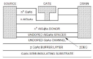
Figure 2. AlGaAs/GaAs HEMT Device Structure [4]
GaAs has property of higher electron affinity as a result of which free electrons are transferred to undoped GaAs layer. GaAs has the electron mobility, at room temperature is more than 5 times larger than silicon, which helps to minimize series resistances and maximum value of electron velocity is about 2 times than that of silicon. Because of some of these reasons, GaAs technology is commonly used wire-less communication and highspeed analog ICs. In this structure, 2DEG layer or two dimensional gas will be formed. The buffer layer job is to avoid scattering. The n type AlGaAs layer of the HEMT is depleted completely through depletion [9]. Electrons traveling vertically will be collected by 2DEG [5]. The most important point about the channel layer in the HEMT and PHEMT devices is the two dimensional electron gas (2DEG) that results from the band-gap difference between AlGaAs and GaAs [4, 5]. The concentration of 2DEG is controlled by the Vgs. Therefore, Vgs is also chosen as a critical parameter to concern in this paper.
HEMT device structure consists of critical parameters that are the sources of noise and their along with channel noise is greater for this structure. The influence of noise is considerable on performance of the device at the different frequencies. Higher noise current can also be seen because of shorter channel length. Noise currents are inversely proportional to channel resistance which in turn to gate length. This is the reason for the need of proper modeling of the devices for different applications.
A low noise amplifier (LNA), which provides modest RF gain at a low noise Figure in RF front end applications. LNA is a key component in the receiving section of communication system. The main objective of LNA is to receive the input signal, which is in general very weak and to amplify besides maintaining minimized noise levels. The performance metrics of this RF front end subsystem are Gain and Noise Figure. In this paper, these two were taken as performance measures and parametric values of device like gate resistance, transconductance besides gate source voltage were considered. Gate Resistance and Gate source voltage are having direct influence on the noise influence on device operation, as the noise current is inversely proportional to the resistance [8].
HEMT LNA is designed using microstrip line methodology and the substrate chosen is FR4, where the dielectric constant value is 4.6. Noise bandwidth is 6 GHz and H =1.6mm, where as W =3.00mm and L = 6.79 mm. The operating voltage is 3v dc. And the Impedance matching networks consists of inductive and capacitive components with terminations of 50 ohms at input and output. The centre frequency of the design is taken as 5.8GHz in accordance with the demands of the communication applications like Software Defined Radio.
The design of MODFET Low noise amplifier Using FR4 Substrate is as shown in the Figure 3.
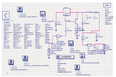
Figure 3. Design of MODFET Low Noise Amplifier Using Fr4 Substrate
In Figure 3. The circuit is developed based on micro strip design methodology [6] and a strip line of 4.6 dielectric constant value is considered with H=1.6mm, W =3.00mm and L = 6.79 mm and the centre frequency is considered to be 5.8GHz. EE_HEMT Model is considered. Operating voltage is considered as 3v dc in both the cases. Impedance matching networks were designed using L and C components with terminations of 50 ohms at input and output. Sweep frequency is considered to be 1 GHz to 10GHz with a step value of 1GHz. The design shown in Figure 2 is also modified with regard to RT Duroid substrate, where the substrate parameters are H = 0.75mm, dielectric constant of 2.2 and Tan value of 0.15mm
In this section, the variation of Gain and Noise Figure w.r.t frequency are shown in Figures 4 & 5. shows the when the gate resistance is of 3.69 ohm with transconductance as 100mS. Noise Figure values are obtained across the sweep range of 1GHz to 10GHz. The gate source voltage is -3v in this combination of parametric values
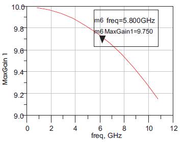
Figure 4. Gain Variation When Rg value is 3.69 ohm, Gm max = 70 mS, IS= 30UA, VGS = -3V
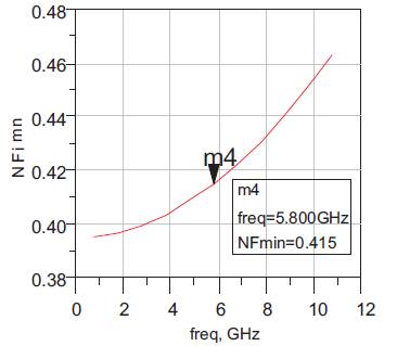
Figure 5 .NF min Variation When Rg value is 3.69 ohm, Gm max = 100 mS, Is= 30UA, VGS = -3V
Figures 6 & 7 shows the variation of gain and Noise, when the gate resistance is of 3.69 Kohm with transconductance as 70mS.
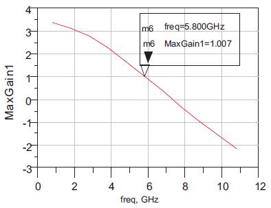
Figure 6. Gain Variation When Rg = 3.69 kohm, gm = 70mS, Id = 30uA, Vgs = -3v
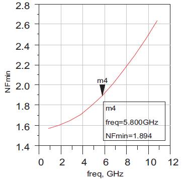
Figure 7. NF min Variation When Rg = 3.69 kohm, gm = 70mS, Is = 30uA, Vgs = -3v
Figures 8 & 9 shows the variation of gain and Noise, when the gate resistance is of 3.69ohm with transconductance as 70mS and Is =15uA.
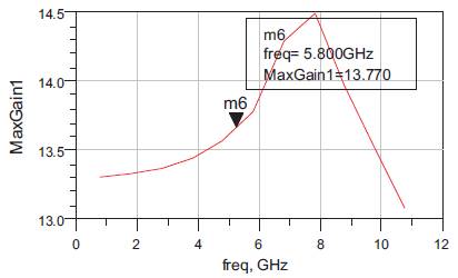
Figure 8. Gain Variation When Rg = 3.69 ohm, gm = 70mS, Is = 15uA, Vgs = -3v
Figures 10 & 11 shows the variation of gain and Noise, when the gate resistance is of 3.69ohm with transconductance as 70mS, where as the gate source voltage is of -1v.
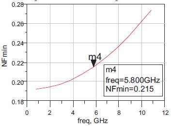
Figure 9. NF min Variation When Rg = 3.69 ohm, gm = 70mS, Is = 15uA, Vgs = -3v
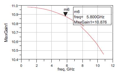
Figure 10. Gain Variation Rg = 3.69 ohm, gm = 70mS, Is = 30uA, Vgs = -1v
Figures 2 & 13 shows the variation of gain and Noise1 Figure, when the gate resistance is of 3.69ohm with transconductance as 70mS
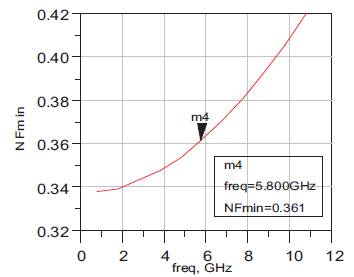
Figure 11. NF min Variation Rg = 3.69 ohm, gm = 70mS, Is = 30uA, Vgs = -1v
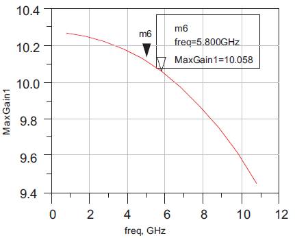
Figure 12. Gain Variation \Rg = 3.69 ohm, gm = 70mS, Is = 30uA, Vgs = -3v
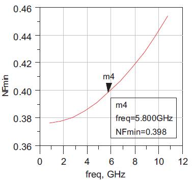
Figure 13. NF min Variation \Rg = 3.69 ohm, gm = 70mS, Is = 30uA, Vgs = -3v
Performance Summary is shown in Table 1. Various conclusions can be drawn from the above results and also from the Table, as the maximum gain value obtained for the PHEMT LNA design is 13.77dB with NFmin having a good range of values between 1GHz and 10GHz. Figure 14. describes the Variation of Gain and NF min for different combinations of parametric values. Another good inference of these results can be the variation in gain and NF value from C1 to C4 i.e. when Is value changes from 30uA to 15uA, which indicates the effect of noise on the performance of the device operation.
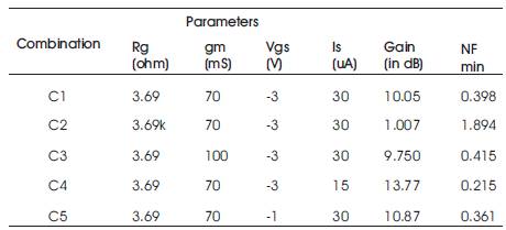
Table 1. Performance comparison of different combinations of parametric values of HEMT LNA
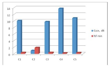
Figure 14. Variation of Gain and NF min for different combinations of parametric values
Similarly, when gm changes also, there is a shift in gain drastically and also in noise figure values. According to the theoretical observations, the typical value of noise figure for a LNA design should be less than 1.5dB, which is well in accordance with the values obtained here, except when Rg is a higher value, which indicates the influence of shot noise. An important conclusion can be drawn here is increased value of gate resistance reduces the gain as it is the source of the shot noise, which is in accordance with the theoretical observations. As the noise influence is more at higher frequencies the main reason for this behavior is once again the shot noise, which is inherent within the device.