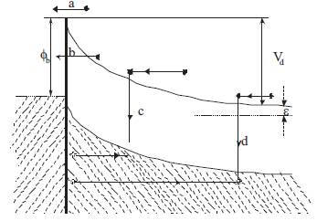
Figure 1. Represents Current Transportation from Semiconductor to Metal at Forward Bias.
The energy band diagram and space charge regions of Schottky barrier (SB) diode are different from normal PN diodes. Many facts and theories must be studied and developed to assist in the understanding and implementation of SB diodes. Few samples of SB devices were prepared by thermal deposition under vacuum then was tested and studied carefully. An interfacial layer was introduced between metal and semiconductor. I-V and C–V were measured, drawn and discussed in details. The current transportation mechanism of the prepared samples was found to be of thermal mechanism type. The current transportation depended on the potential barrier height. From C–V characteristics, it was found that the potential barrier height was decreased as the interfacial oxide becomes thicker.
Schottky barrier (SB) diodes have many electronic properties; some of them are shared with normal PN junction, such as structure and potential barrier. Others are different such as energy band diagram and space charge region that formed at semiconductor side. In addition, potential barrier height is usually less than energy gap of semiconductor, and current transportation mechanism of SB is due to thermal emission. For all these reasons many facts and theories have been developed and implemented to assist in the understanding of Schottky barrier behaviors [1, 2, and3] when used as a solar cell [4, 5, 6 and7] or as a photo detector [8, 9 and 10]. Schottky barrier can be used to detect ultraviolet, visible and infrared rays. The structure of SB is suitable for short wavelength detection; this is due to current transportation carried out by the majority carriers and not to generationrecombination process as in normal PN junctions. Another advantage of SB diode is that it is easy to fabricate with low break down voltage and high leakage current [11].
Generated gap states are found in all Schottky barrier diodes. They are moved from the accepter level near the top of valance band to the donor level underneath the conduction band. It is evident now that an interfacial layer has formed between metal and semiconductor. This model suggested that the formation of such gap states is due to chemical defects (oxide layer) or the dangling bonds. If the oxide is very thin the electrical properties of the junction are the same as normal or Schottky barrier in which the electron can tunnel through the thin oxide layer. The potential barrier height in MIS structured depends very strongly on the type and thickness of the oxide layer. It is proved that the barrier height is inversely proportional with oxide thickness [12 and 13].
Figure 1. Represents Current Transportation from Semiconductor to Metal at Forward Bias.
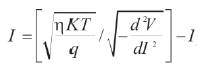
Figure 1 represents the current transportation mechanisms [14]. From semiconductor type (n) to metal in metal-semiconductor (n) junction they can be represented by four types: (a) Thermal electron emission (b) Tunneling through potential barrier, (c) recombination at space charge region and (d) recombination at the neutral zone (carrier injection) [14]. Type (a) current transportation is the most important mechanism, and current density (Jsat) due to this mechanism is given by:
Where A* is the effective Richardson constant, K is the Boltzmann constant T is the temperature in Kelvin, q is the electric charge and φB is the potential barrier?
If forward bias voltage (V) is applied, current density (J) Becomes
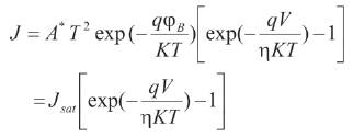
Where η is the ideality factor? If η=1equation (2) becomes ideal equation in which thermal electron emission is the dominant mechanism for current transportation. However if η >1 that means the diode behavior deviates from the ideal behavior. Determination of the ideality factor value is very important to calculate the potential barrier height. But as the effect of series resistance starts to appear, determination of ideality factor becomes difficult. For Schottky, diode has a series resistance (Rs) which is in parallel with the leakage resistance (Rj) the current can be given as follows [3]
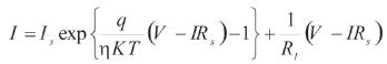
If a forward voltage is applied, the value of reverse saturation current is very small and can be neglected. If T, η, Rs and Rj are considered to be constants, then I can be given as follows
If I drawn against  η is the slope of the curve and Is
is the intersection with I axis.
η is the slope of the curve and Is
is the intersection with I axis.
Practically [15] if an oxide is found between metal and semiconductor, two groups of gap states will exist. The first group, which accumulates between the semiconductor and oxide, will be in equilibrium with the second group that exists near metal. The current transportation mechanism for MIS structure is attributed to the spacecharge limited current. The electrons injected from semiconductor toward the metal, will suffer from trapping due to the existence of free traps in the oxide. The current decreases if the injected electrons are less than the thermally generated electrons (n). This means that the ohmic mechanism is responsible for the current transportation.
The ohmic current (Jo) can be expressed as follows [16]

Where µ is the electron mobility and d is oxide thickness. However, if the number of injected electrons is greater than thermally generated electrons, the effects of space charges will appear and current (Jc)
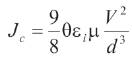
Where θ is the rate of free charges to the total charges and εi is the oxide permittivity. The transition from ohmic region to space charge region occurs at the transition voltage (VT) which is given by

Beyond the space charge region, all the traps are filled,
and the current increases very quickly according to the
relation  Voltage at which current increases quickly
is called the trap filled limit voltage (VTFL) and it can be given by:
Voltage at which current increases quickly
is called the trap filled limit voltage (VTFL) and it can be given by:
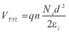
Where NT the trap concentration. Again beyond this region (the trap filled limit region), the current increases linearly with voltage, and it can be expressed as given by equation (6). Figure 2 shows the I-V characteristic for all regions mentioned before [16].
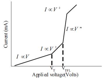
Figure 2. Shows the I-V characteristics for all regions forward bias.
In order to investigate and discuss the high-speed responsivity of Schottky barrier and potential barrier height, the capacitance of the junction must be introduced and measured. It is well known that the dominant capacitance in normal diodes is the diffusion capacitance. But no such capacitance in Schottky barrier diodes has been found, and this is the reason why these diodes have a very high speed of responsivity. When a negative voltage is applied on the metal side the energy band will bend upward. Holes, which are the majority carriers, will accumulate at the surface between semiconductor and oxide and it is known as the accumulation region. However, if positive voltage is applied, the holes will be depleted from the interfacial layer, and that will make the energy band bend downward. It is called the inversion region, where the minority carriers (electrons) accumulate to form an inversion region.
In this research, many samples of Schottky barrier MOS structures were prepared by thermal deposition under high vacuum using Balzer coating unit. Deposition parameters and sequence of fabrication MOS devices are as follows
All samples prepared in this research for different parameters are shown in Table 1. The samples were circles of 0.2 cm2 area.
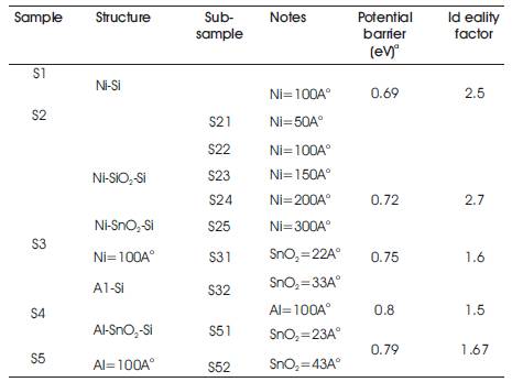
Table 1. The Prepared Samples of Different Structures with Potential Barrier and Ideality Factor
Figure 3 shows I-V characterictic of Shcottky bariar (S1 and S22) for forward and reverse biased voltages. It is clear that the reverse current is nearly constant while the forward current increases as the voltage increases. This is evidence that the potential barrier, formed for the current, is to be rectified. For the voltage “between” 0.1 to 0.4 volt, the current increases very rapidly. In order to know the current transportation mechanism, the ideality factor must be calculated using equation 9 as follows [18].
The term between the brackets  represents the
slope of the curve In I versus V. Ideality factors of all
samples were calculated and tabulated in Table 1.
represents the
slope of the curve In I versus V. Ideality factors of all
samples were calculated and tabulated in Table 1.
The ideality factors of S1 and S22 were 2.5 and 2.7 respectively. These results indicate that the current transportation mechanism for this range of voltages is the recombination at the surface between metal and semiconductor. The value of ideality factor of S22 is higher than the ideality factor of S1 due to the native oxide formation, which lowers the potential barrier height.
Prior the study of oxide thickness effect, the effect of metal thickness must be studied and optimized. Nickel thickness is varied and the I-V characteristic of S2 is shown in Figure4.
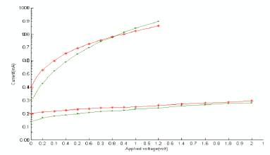
Figure 3. I-V characteristic of Schottky barrier (S1 and S22) for forward and reverse
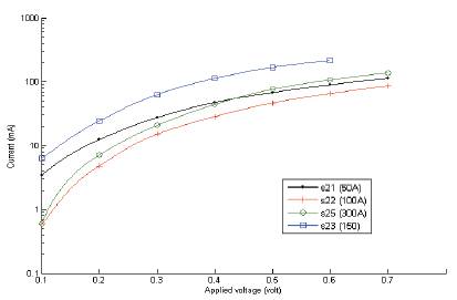
Figure 4. I-V characteristics of samples S21, S22, S23 and S25
For voltage less than 0.4 volts, the ideality factor has two values. It is 2.7 for S21, S23, and 1.6 for S22 and S24 samples. The first value indicates that the current transportation mechanism is the recombination while it is thermal emission mechanism for the second value. For high voltage (higher than 0.4 volts), the effect of series resistance appears in all samples to saturate the currents.
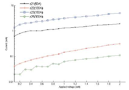
Figure 5. Reverse I-V characteristics of samples S21, S22, S23 and S25
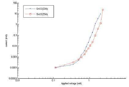
Figure 6. Forward I-V characteristic of samples S31 and S32
The reverse I-V characteristics of the same samples are shown in Figure 5. The reverse current in all sample were very small and nearly constant which means that the rectification in these samples was performed.
The sample of 100Ao nickel was chosen due to its good rectification properties. The type and thickness of the oxide were changed. Forward I-V characteristics of samples S31 and S32 of different SnO2 oxide are shown in Figure 6. For the voltage range from 0.1 to 0.4 volts, the relation between current and voltage was linear. This means that the density of injected free carriers is less than the density of thermally generated free carriers, for this reason the ohmic conduction is responsible for current transportation as it is represented by equation 5. When the voltage is increased above than 0.4 volts, the current transportation will change from ohmic mechanism to space charge mechanism in which the injected current density is bigger than the density of thermally generated carrier. The current can be represented by equation 6. As the voltage is increased up to 1m volt the current increases very rapidly due to filling all traps. This voltage is called the trap-filled limit voltage and it can be expressed by equation 8.
The reverse characteristic of S3 is shown in Figure 7. The reverse currents in all samples are the same, but they didn't show saturation, and this is due to the potential barrier height that depends on the voltage applied. The reverse current increases as the thickness of the oxide decreases due to the tunneling effect that has already been noticed [19].
Figure 7. Reverse I-V characteristic of S31 and S32.
The type of metal is changed and the aluminum is used for the following samples. Figure 8 shows the forward I-V characteristics of S4 and S5. In sample S4 there are two regions, the first at forward voltage less than 0.4 volts, at which the current transportation mechanism is thermionic emission. The electron emitted above the potential barrier, is formed at the interfacial layer and the ideality factor is 1.5. The second region is at the forward voltage higher than 0.4 voltages, when the series resistance starts to affect the current transportation mechanism. The current in sample S5 increased gradually which means the current transportation mechanism is thermionic emission at all times and the ideality factor is about 1.67. The reverse current for sample S4 is nearly constant which gives good rectifying properties, while at sample S5 the reverse current didn't saturate which means that the reverse potential barrier depends on the applied voltage and does not give good rectifying properties.
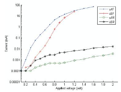
Figure 8. Forward and reverse biased I-V characteristics of S4 and S5
When a comparison is made between the different structures, two points are noted. At foreword voltage sample, S3 obeys the space charge limited current law. At the other point, at reverse voltage it can be seen that the current increases in S4 due to the reduction of the potential barrier height. While in sample S3 the current increases as the oxide thickness increases due to tunneling between semiconductor and metal [16].
In order to evaluate the internal potential barrier height obtained from the I-V characteristics, C-V characteristic should be studied. The internal potential barrier (Vbi) can be calculated from C-V curve, where Vbi represented by straight line that intersects with the voltage axis. Figure 9 represents C-V characteristic of sample S32 at frequencies of 10 and 100 kHz. The three regions appeared very clearly at this fig. as it has already been mentioned. At forward voltage higher than 0.7 volts, the capacitance is flattened and it depends on the applied voltage, but the flat was lowered as the frequency increased. This region is the so-called accumulation region. The second region appeared at the reverse bias in which the capacitance depends on neither voltage nor frequency. This region is the inversion region. The third region falls between the accumulation and inversion regions. It is called the depletion region. In this region, the voltage increases linearly with voltage.
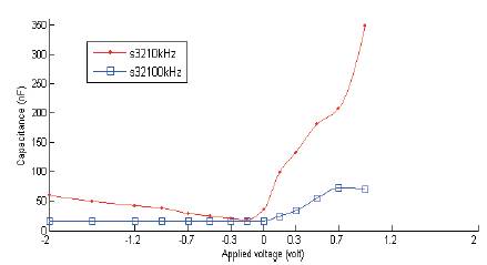
Figure 9. Represents the C-V characteristics of sample S32 at 10 & 100 kHz
Figure 10 represents the C-V characteristics of sample S5 (Al-SiO2-Si) at 10 KHz frequency. It is clear that this sample behaves in the same way that sample S33 behaved in the previous Figure. There are two exceptions: first there are two regions, inversion and depletion regions but there is no accumulation region. The second difference is that the capacitance in these samples increases much more rapidly with voltage at the depletion region than it has been shown in the previous Figure. This result indicates that the density of interfacial states is high in nickel sample compared with the low density of interfacial states in aluminum samples.
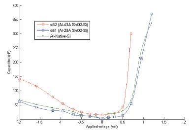
Figure 10. Represents the C-V characteristics of sample S5 (Al-SiO2-Si) at 10 kHz
The internal potential barrier of all samples was calculated and listed in Table 1. It is clear that the potential barrier height decreased as the thickness of oxide increased. It is also noticed that the potential barrier height of aluminum samples is bigger than the potential barrier height of nickel samples.
I-V characteristics of MIS samples show that at forward voltage there are three distinct regions. The first region, which appears at low voltage, is called the Ohmic region. The second region, which appears at medium voltage, is called the space charge region. At the third region, the current increases very rapidly with voltage, because all traps are filled. On the other hand, at reverse voltage, the current did not saturate but continuously increased. The increase in current is due to different reasons: For thin oxide, the increment is due to tunneling between semiconductor and metal. However, for thick oxide, the current increases due to the reduction of potential barrier height.
The C-V characteristics depict also three regions: these are inversion region at reverse biased; accumulation region at high forward voltage, and between these two regions, depletion region exists.