Abstract
Arithmetic Logic Units (ALUs) are very important components in computer systems. They are digital circuits utilized to perform a wide variety of arithmetic and logic operations. Modern Central Processing Units (CPUs) contain powerful and complex ALUs. One such operation performed by ALUs is that of Multiplication. Multiplication scales one variable by another. This research involves the design, implementation and verification of a 4-digit BCD Multiplier Core with Similarity Investigator for path delay reduction. The system is implemented using Xilinx ISE 14.7, verified using ISim and Digilent Nexy3 toolkit and was utilized as the development platform. The research concluded that similarity investigation was capable of path delay reduction of up to 97% compared to that when no similarity investigation was applied. The system can conduct a maximum of 889 unique multiplication operations before facing diminishing returns as a result of the similarity investigation search procedure.
Keywords:
- Arithmetic Logic Unit
- Binary Coded Decimal
- BCD Multiplier
- BCD Multiplication
- Similarity Investigation
Introduction
Multiplication is a fundamental arithmetic operation. Kumar et al. (2012) claim that multiplication accounts for more than 70% of Instructions in microprocessors and most digital signal processing algorithms. Binary Coded Decimal (BCD) multiplication is vital in electronic computing. According to a survey by Tsang and Olschanowsky (1991), 55% of columns of numeric data were decimal data types, and 43.7% were integer data types, which could be stored as decimals. Cowlishaw (2003) also notes that finance, commerce, statistics, and internet-based applications require precise rounding methods, which are often imposed by law
BCD multiplication is more complicated than binary multiplication. Each BCD digit is represented by four bits. Invalid BCD digits, bit carries, and digit carries must also be taken into account in the multiplication process. BCD operations are inherently time-consuming and area intensive. However, BCD multiplication cannot satisfy high-performance applications that require high precision and accuracy, as many fractional numbers cannot be represented exactly in binary with a finite number of bits. Decimal operations initially used software algorithms based on binary arithmetic. These schemes were often three to four orders of magnitude slower, as noted by Cowlishaw (2003). Véstias and Neto (2011) suggest that the use of dedicated hardware circuits can improve the performance of decimal arithmetic operations.
This paper involved the design and VHDL implementation of a 4-digit BCD multiplier core on the Digilent Nexys3 toolkit, capable of validating inputs to avoid multiplication of invalid BCD digits, validating operands to avoid trivial multiplications by ones and zeros, and reducing path delay of multiplication operations using similarity investigation. The design was based on parallel PPG by the accumulation of a sequentially shifted multiplicand.
The main objectives of the research are,
1. Review of Existing BC Multiplier Systems
Ahmed et al. (2018) presents a digit-by-digit decimal multiplier with stages of Partial Product Generation (PPG) and Partial Product Reduction (PPR). A BCD Digits Multiplier (BDM) block generates partial product values with a binary multiplier and a High Performance Partial Product Binary to Decimal (PPBD) converter. Area and delay at the PPG stage are excessive since partial products are converted from binary to BCD, as noted by Ahmed et al. (2018). Anguraj and Krishnan (2021) reduced the time delay and area requirements of the work done by Ahmed et al. (2018) at the PPG stage with a modified BDM block.
The modified block generates binary partial product values using a constant multiplier and a PPBD converter (Anguraj & Krishnan, 2021). Considerable time delay still remains at the binary-to-BCD conversion stage of the PPBD converter block. Sreelakshmi et al. (2019) present a VBCD multiplier using 3:2 VBCD compressors to reduce delay and stages of partial product addition. The Vedic methods support parallelism using a divide-and-conquer approach. The Vinculum number system reduces complexity by using [0, 5] for decimal [0, 5] and [-4, -1] for decimal [6, 9]. Four-digit multiplicands and multipliers are divided into two-digit numbers using the Vedic Urdhav- Triyakbhyam method. A LUT-based one-digit VBCD multiplier reduces processing time as all partial products are saved in memory. Two-digit multipliers generate four partial products, which are summed in parallel by compressors (Sreelakshmi et al., 2019). There are no carry propagations; however, considerable hardware is used to modularly implement digit-by-digit multiplication.
The paper by Sworna et al. (2018) presents a novel N×M digit BCD multiplication algorithm which uses 1x1-digit BCD multipliers based on five heterogeneous LUTs. To sum the partial products, the BCD adder circuit proposed by Haque et al. (2018) was used in the final multiplication step. This approach eliminates the conventional stages of recoding, PPG, PPR, and BCD conversion, which leads to a reduction in overall area and delay. However, it should be noted that increasing hardware utilization with scaling may lead to diminished returns.
Aruna and Bhanumathi (2018) proposed an optimized BCD multiplier architecture that includes area and power reductions for binary product computations and higher to speed during binary-to-BCD conversion. Binary products are generated using a multiplier stage adapted from Castillo et al. (2017), with the complexity being reduced by limiting multiplications to valid BCD digits. They also proposed a modified binary-to-BCD converter architecture based on the Shift-and-ADD-3 algorithm. The ADD-3 module's LUT is generated and mapped with a shifting algorithm module to reduce area and delay. However, there are still significant latencies at the binary to- BCD conversion stage based on the Shift-and-ADD-3 algorithm.
The BCD multiplier presented by Lakshmi et al. (2016) is based on Vedic Mathematics, utilizing Vinculum methods to reduce carry generations and carry propagations. A multiplier and multiplicand correction unit is used to convert decimal numbers to Vinculum numbers, which are then multiplied with one-digit multipliers through AND gates. A XOR gate checks the sign bit of the generated partial products, which are then passed through a complement circuit or directly to a BCD adder using a 2:1 MUX depending on the sign bit. However, the multiplier and multiplicand correction unit and BCD adder blocks result in considerable path losses, and the pipeline is delayed from iterative digit-by-digit algorithms.
Kumar and Umadevi (2015) presented a modified combinational parallel BCD multiplier. They used radix-10 recoding for signed-digits of the set [-5, 5] and coded a positive set of multiplicand multiples in XS-3. The use of signed digits reduced combinations and enabled the generation of multiples using bit inversions. Decimal products were obtained from stages of PPG, generation of multiplicand multiples, and radix-10 recoding of operands to ODDS with four-bit binary encoding. Partial products were reduced after recoding using a bank of ripple carry adder trees and then converted to a nonredundant BCD product. Kumar and Umadevi (2015) proposed a BCD quaternary tree adder for the final BCD conversion. A carry prefix tree computed decimal carries, and four-bit digit adders computed two-conditional BCD digit sums. However, the quaternary adder delay exceeded that of a binary adder with a similar topology. Increased scaling diminished the delay and hardware utilization improvements.
Mehta et al. (2013) proposed an NxN-BCD multiplier scaled from 1x1 VBCD multipliers, incorporating a modified binary-to-BCD converter. The N-even decimal digits are equally partitioned, and Vedic Urdhva- Tiryagbhyam multiplication is performed, followed by BCD adders generating the final output digits. The Vedic Urdhva-Tiryagbhyam method increases multiplication efficiency by reducing hardware circuitry overhead, and a divide-and-conquer approach reduces delay during multi-digit multiplication (Mehta et al., 2013). The main contribution of Mehta et al. (2013) lies in the modified binary-to-BCD converter, which was based on an algorithm by Bhattacharya et al. (2010). However, this algorithm was later optimized by Al-Khaleel et al. (2011), leading to errors in special cases. The system developed by Mehta et al. (2013) experiences substantial delays from stages of binary computation and BCD conversion.
Al-Khaleel et al. (2012) introduced a delay-optimized 4x4- BCD multiplier architecture that directly manipulates BCD numbers using simplified Boolean expressions, thus avoiding binary conversions. Since a product is eight bits wide, there are 256 possible combinations, but only 100 of them are valid. Implementing the output expressions requires a hierarchy of six-input LUTs (Al-Khaleel et al., 2012). However, as the number of digit operands increases, the number and complexity of output expressions also increase. This, in turn, requires a larger hierarchy of LUTs and drastically increases hardware utilization.
A parallel-serial decimal multiplier is proposed by Dadda et al. (2012). The multiplicands are asserted in parallel onto a linear array. Multipliers are asserted in digit-serial form. Multiplication of the linear array by a multiplier digit generates a partial product. A multiplication array is partitioned into sub-arrays. The sub-arrays are populated by partial products. Sub-arrays are summed in, to produce the binary product. The binary product is then converted to BCD (Dadda et al., 2012). The proposal by Dadda et al. (2012) reduced the complexity and exploited overlapping updates for speeding up the pipeline. Substantial delay still exists during the binary-to BCD conversion stage. Moreover, resource requirements are intensive with increased input width.
Guardia (2012) presents a fully pipelined decimal multiplier based on– recoding multiplier operands in SD radix-10, a simplified PPG, and decimal adders. Multiplicand multiples are computed and coded into BCD-4221. A SD radix-10 unit recodes each BCD-8421 multiplicand digit between [-5, 5] using five-bit signed magnitude in parallel. The recoded multiplicand and computed multiplicand multiples are multiplied digit-by digit. PPG is reduced by decimal adders and CSA techniques. This compresses the partial products tree which are coded into a reduced group of BCD-4221 (Guardia, 2012). The main drawback of this design is the BCD-8421 coding and introduces a computational cost from corrections in the decimal reduction CSA.
Vazquez and Dinechin (2010a) presents an area-efficient pipelined method of implementing BCD multiplication on six-input LUT FPGAs. Parallel implementations accelerate binary multiplication with deeper pipelines. The proposed architecture is based on decimal PPG using SD radix-5 recoding of multiplier operands. Only 2X multiples are precomputed. The remaining BCD multiplicand multiples are computed in a decimal PPG block (Vazquez & Dinechin, 2010a). PPR is performed by a tree of BCD carry ripple adders. The design by Vazquez and Dinechin (2010b) employs novel binary multiplication which adds latencies during data type conversions.
Véstias and Neto (2010) proposed an architecture for decimal-to-binary conversion, which utilized existing coarse-grained embedded binary arithmetic blocks to develop architectures for 8x8 and 16x16 parallel BCD multipliers. The BCD operands were subdivided and converted to binary using direct calculation of the decimal number with Horner's rule applied to binary arithmetic. The PPG stage utilized binary multipliers, which were reduced to addition of shifted values. Inner products were summed in binary and then aligned to form partial products. These partial products were converted to decimal using the Shift-and-ADD-3 algorithm, and the final product was obtained through a final addition (Véstias & Neto, 2010). However, the stages of decimal-to-binary and binary-to-decimal conversions increased hardware utilization and induced substantial delays.
Sutter et al. (2009) presented sequential and combinational techniques for implementing digit-by digit decimal multipliers, which were scaled from 1x1 multiplier units. The first technique was based on the work by Jaberipur and Kaivani (2007) and involved binary multiplication with a post-correction stage. Binary-to-BCD conversion was achieved through binary sums of correcting terms. The BRAM (Block RAM) based multiplier was synchronous and preferred for sequential and pipelined implementations. In the design proposed by Sutter et al. (2009), the products of four-bit operands were mapped into a 28x8-bit ROM implemented with LUTs. Additionally, the final technique introduced a MUX-based cell for combinational multipliers. The design included a low-level definition of components and utilized an array of multi-input LUTs. However, the first technique suffered from considerable latency due to the binary-to-BCD conversion stage, while the latter techniques exhibited significant hardware utilization that increased with the operand size.
Veeramachaneni and Srinivas (2008) presented a novel parallel architecture for a 32-digit parallel tree-structured BCD multiplier. The architecture employed various components such as novel binary counters, BCD full adders, and binary-to-BCD converters. Digit-by-digit multiplication was implemented using an array of 4x4 binary multipliers, generating an array of eight-bit binary numbers. These binary numbers were added using binary counters based on advanced look-ahead techniques. The results were further summed using lower-order counters and then individually passed to a set of binary to- BCD converters.
The binary counters added the partial products using a PPR (Parallel Prefix Reduction) tree, and binary-to-BCD conversion was performed at significant stages of the computation. The resulting BCD numbers were then added with BCD adders. Correction logic blocks were employed to compute the BCD equivalent of the eight-bit binary numbers. The operations performed in this architecture ultimately resulted in four 32-digit BCD numbers, which were further processed through BCD adders to obtain the final product (Veeramachaneni & Srinivas, 2008). It is important to note that continuous binary-to-BCD conversions and the manipulation of both binary and BCD representations in this design led to increased hardware utilization, latency, and complexity.
Neto and Vestias (2008) proposed a novel BCD multiplier architecture based on binary arithmetic. Embedded binary multipliers in FPGAs are exploited and a novel approach towards binary-to-BCD conversion is proposed. A BCD-to-binary converter calculates the binary operands. Powers of ten are calculated as a sum of powers of two. Binary operands are passed through embedded multipliers which generates a binary final product. Binary final products are iteratively converted to base-1000 by applying Horner's rule LSD first. Each base- 1000 digit is then converted to BCD with the Shift-and- ADD-3 algorithm (Neto & Vestias, 2008). The BCD-tobinary and binary-to-BCD conversion steps significantly reduce efficiency. Larger BCD multipliers also require more sub-units which increase area and latency.
2. Design of the Overall 4-Digit BCD Multiplier System
The 4-digit BCD multiplier system consists of five inputs and three outputs, as depicted in Figure 1 of the FSM-D interface definition. The inputs include "clk," which is a periodic clock waveform that drives the system. When the "reset" input is set to a HIGH state, the entire system is initialized, and the default state is enforced. On the other hand, when the "start" input is set to a HIGH state, the system begins the multiplication process by multiplying the values of A (multiplicand) and B (multiplier). The result of the multiplication is then presented at the output "final product," and the output signal is set to a HIGH state, indicating the completion of the process. In cases where the system memory reaches its capacity, the "overflow" signal is set to a HIGH state.
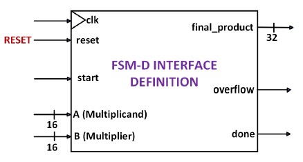
Figure 1. FSM-D Interface Definition of the Overall 4-Digit BCD Multiplier System.
The datapath design of the overall 4-Digit BCD multiplier system, depicted in Figure 2, consists of four blocks. Block 1 is the Validator, which serves as the frontend to the Similarity Investigator. The operands A and B enter the Validator first, where its validity is checked. The Validator determines the validity of both operands and generates a decision at the output "decision" based on this information. If either operand is found to be invalid, the "fault" signal is asserted HIGH; otherwise, it is asserted LOW.
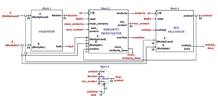
Figure 2. Datapath Design of the Overall 4-Digit BCD Multiplier System
Validated operands then pass through the Similarity Investigator in block 2. The Similarity Investigator acts as the frontend to the BCD Multiplier. It searches an internal RAM for a previous multiplication involving operands A and B. When a match is found, the output "similarity" is asserted HIGH, and the saved product is issued at the output "msi_product". When no match is found, the output "similarity" is asserted LOW, and the output "msi_product" is padded with zeros. The signal "check_similarity_done" is then asserted HIGH, indicating the end of the process. If no match is found, the BCD Multiplier in block 3 proceeds to multiply operands A and B. The result is issued at the output "product" and saved in the RAM of the Similarity Investigator. The signal "overflow" is asserted HIGH only when the RAM is full. The signal "multiply_done" is then asserted HIGH, indicating the end of the multiplication process. The Multiplexer in block 4 selects the "final_product" between the outputs of the Validator, Similarity Investigator, and BCD Multiplier. The selection depends on the status of the "fault" and "similarity" signals.
The datapath interface definition of the 4-Digit BCD Multiplier system is based on the datapath design of Figure 2. A controlpath interface definition was developed using the datapath interface definition and the FSM-D interface definition of the 4-Digit BCD Multiplier system. Both datapath interface definition and controlpath interface definition were combined to construct the FSM-D model for the 4-Digit BCD Multiplier system as shown in Figure 3.
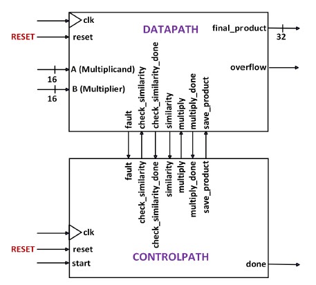
Figure 3. FSM-D Model for the Overall 4-Digit BCD Multiplier System.
State transitions of the controlpath were analyzed by following the desired sequence from the operation of the datapath design. A state diagram for the controlpath of the 4-Digit BCD Multiplier was then constructed and can be seen in Figure 4
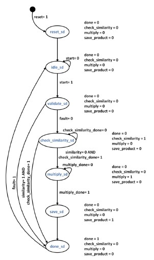
Figure 4. State Diagram For Control path of the Overall 4-Digit BCD Multiplier System.
2.1 Design of Validator Architecture
The Validator serves as the frontend component to the Similarity Investigator and is responsible for determining the validity of the input operands for the multiplier system. It checks if the operands are either invalid BCD digits, valued zero, or one. An operand is considered invalid when a BCD digit exceeds X"9". Trivial multiplications occur when the operands are valued zero or one. These three events are interpreted as faults by the Validator. Figure 5 provides the FSM-D interface definition for the Validator.
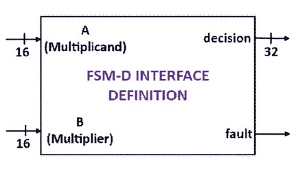
Figure 5. FSM-D Interface Definition For Validator.
When a multiplication involves an invalid BCD digit, the decision made by the Validator is the error code X"DEEFDEEF". This error code corresponds to a seven segment display of "Err Err". Multiplication by zero yields a decision of zero, and if one of the operands is valued one, the decision is simply the value of the other operand. In all these cases, the fault port is asserted HIGH, indicating a fault condition. This immediately displays the Validator decision and prevents further stages of similarity investigation and multiplication. When no fault occurs, the fault port is asserted LOW. At this point, the similarity investigation stage begins, and the decision is formed by concatenating the values of A (multiplicand) and B (multiplier).
2.2 Design of Similarity Investigator Architecture
The FSM-D interface definition of the Similarity Investigator, depicted in Figure 6, includes seven inputs and four outputs. The input "clk" represents the periodic clock waveform for the system. When "reset" is asserted HIGH, the system is initialized, and the default state is enforced. Upon asserting "check_similarity" HIGH, the system searches its internal RAM block for a matching instance of inputs A (multiplicand) and B (multiplier). If a match is found, “similarity" is asserted HIGH, indicating the presence of a similarity. In this case, the saved product is issued at the output "msi_product."
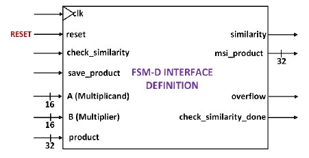
Figure 6. FSM-D Interface Definition For Similarity Investigator Architecture.
Similarity remains LOW when no instance was found and the output msi_product is padded with zeros. check_similarity_done is asserted HIGH at the end of the process. The input product is the result after multiplication of A and B. The system saves the instance of A, B, and product when save_product is asserted HIGH. Previously saved instances are overwritten when exceeding RAM space. overflow is asserted HIGH which indicates that RAM is at capacity. The datapath design of the Similarity Investigator depicts Figure 7 which consists of six blocks. Block 1 is a Hold Register in PIPO configuration. When load is asserted HIGH the Hold Register stores data from input datain. Storing the inputs stabilizes data to the Similarity Investigator from possible change. Stored data is output in parallel to the input datain of the RAM Block in block 5 as shown in Figure 7.

Figure 7. Datapath Design for Similarity Investigator Architecture
The capacity of the RAM Block determines the number of memory locations it can hold. In this case, a capacity of 256 was chosen, as it is a power of two. To traverse the RAM Block, a Modulo (256) Counter is used. In block 2, the Modulo 256 Counter increments by one when the "write" signal is asserted HIGH. The data output from this counter is used as the address input (addressX) for the RAM Block. The data present at the RAM Block input (datain) is then written to the memory location specified by addressX. When the counting process of block 2 is complete, and the RAM Block is at capacity, the "overflow" signal is asserted HIGH. This indicates that data will be overwritten as the counting process restarts.
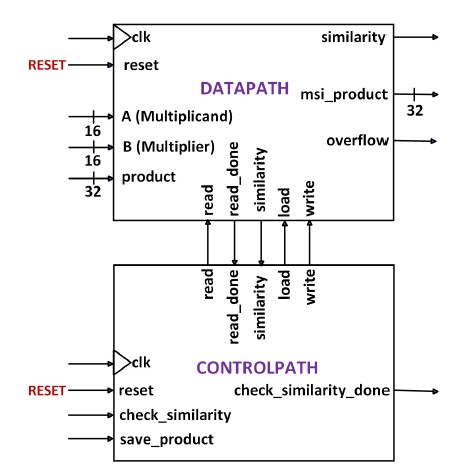
Figure 8. FSM-D Model for Similarity Investigator Architecture.
When the "read" signal is asserted HIGH, the Modulo 256 Counter in block 3 exits the reset state. Block 3 increments by one every clock cycle, and the data output (dataout) from block 3 is used as the address input (addressY) for the RAM Block. The RAM Block performs a self-search for a saved instance of operands A and B at the memory location specified by addressY. The search is based on the concatenation of A and B, which is compared against the upper half of the saved data in the RAM Block, as shown in Figure 9. If a matched instance is found, it is output from the RAM Block as dataout. If no matched instance is found, zeros are output. The lower half of dataout forms the msi_product, while the upper half enters the Comparator in block 6.
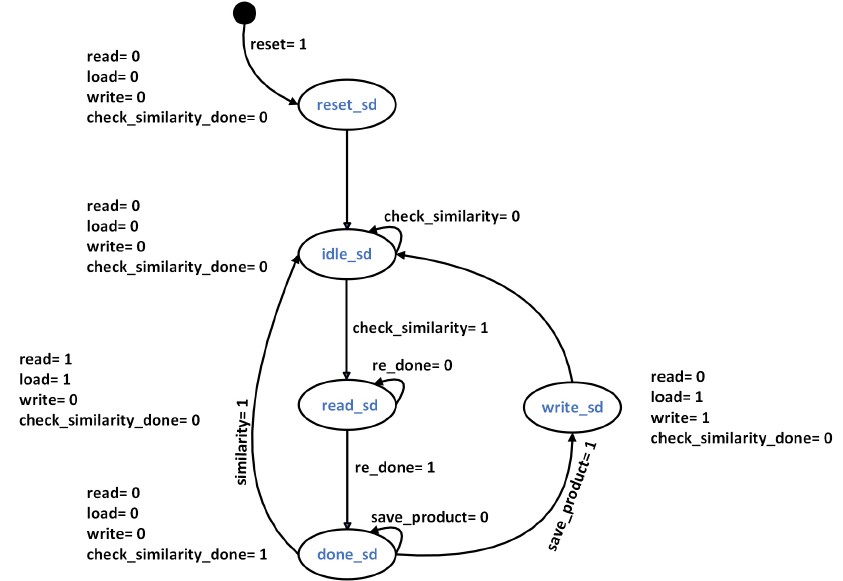
Figure 9. State Diagram for Control path of Similarity Investigator Architecture
A Comparator in block 6 is responsible for comparing the upper half of the RAM Block's dataout with a concatenation of the entered operands. Similarity is only asserted HIGH when the comparison results in a match. In block 4, another Comparator compares the dataout of block 2 with the dataout of block 3. When the comparison matches, the output of block 4 is asserted HIGH. The re_done signal is asserted HIGH when either block 4 or block 6 outputs are HIGH. This indicates the end of the reading process and bounds searches up to the last written memory location.
State transitions of the control path were analyzed by following the desired sequence from the operation of the datapath design. A state diagram for the controlpath was then constructed as shown in Figure 9.
2.3 Design of BCD Multiplier Architecture
Let index be the decimal place of a discrete digit in a compound decimal number and let index be the number in an N-digit wide compound decimal number. The product of arbitrary A and B is given by the algorithm in Equation (1).
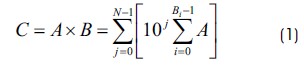
Figure 10 presents the FSM-D interface definition for the BCD Multiplier, which includes five inputs and two outputs. The input "clk" represents the periodic clock waveform that drives the system. When the "reset" signal is asserted HIGH, the entire system is initialized, and the default state is enforced. Upon asserting "multiply" HIGH, the system performs the multiplication operation on the inputs A (multiplicand) and B (multiplier). The resulting product of multiplying A by B is issued at the output "product." Finally, the signal "multiply_done" is asserted HIGH, indicating the completion of the multiplication process.
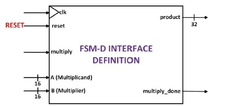
Figure 10. FSM-D Interface Definition for BCD Multiplier (Product Calculator).
The datapath design of the BCD Multiplier, also known as the Product Calculator, consists of seven blocks, as depicted in Figure 11. The operands A and B are stored in the Hold-Shift Registers, specifically in block 1A and block 1B, respectively. When the signal "load_operands" is asserted HIGH, the operands entered at the "datain" ports of block 1A and block 1B are stored. The data stored in block 1A is 32-bits wide, as it accommodates the maximum possible product of 32-bits.
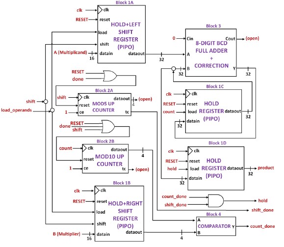
Figure 11. Datapath Design for BCD Multiplier Architecture
The operand A (multiplicand) is initially padded with zeros to form the least significant 16-bits of the data stored in block 1A. The output "dataout" of block 1A is connected to the input "A" of the 8-Digit BCD Adder in block 3. Figure 12 provides an illustration of the design of the 8-Digit BCD Adder, which comprises eight cascaded BCD Adder Units with a +6 correction. Upon reset, inputs A (block 3) and B (block 3), as well as the output "Y" of block 3, are initialized to zero.
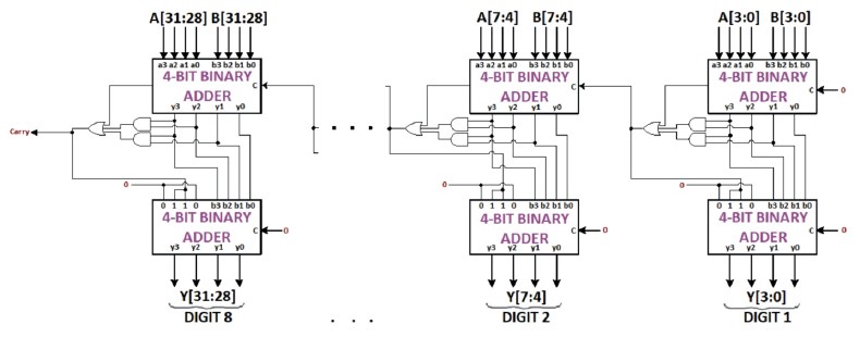
Figure 12. 32-Bit BCD Adder (Source: Bayrakci & Akkas, 2007)
During the first round of addition, the result is A (block 3), which is output at "Y." The output "Y" is then connected to the input "datain" of block 1C, which functions as a Hold Register in a PIPO (Parallel-In, Parallel-Out) configuration. Block 1C stores the current sum when the "count" signal is asserted HIGH. The output "dataout" of block 1C serves as an addend to block 3, resulting in an accumulation loop. The output "dataout" of block 1B represents the least significant nibble of B (multiplier).
The size of accumulation is determined by dataout of block 1B. Block 2B is a Modulo 10 Counter that tracks the size of accumulation. Each instance of count HIGH increments block 2B by one unit. The Comparator in block 4 compares dataout of block 1B with dataout of block 2B. count_done is asserted HIGH when the comparison is equal. This event arrests the current accumulation.
Block 1A performs a left-shift operation on the data by one nibble, while block 1B performs a right-shift operation by one nibble. When the "shift" signal is HIGH, block 2B is reset, initiating a new accumulation process after shifting. The Modulo 5 Counter in block 2A keeps track of the number of shifts. Each occurrence of the "shift" signal being asserted HIGH increments block 2A by one unit. The signal "shift_done" is then asserted HIGH after five increments, indicating the completion of the shifting operation
When both "count_done" and "shift_done" are asserted HIGH, the signal "hold" is set to HIGH. This signifies the end of the multiplication process. The final sum is latched onto the Hold Register in block 1D, which is then outputted as the product. Block 2A and block 2B are reset to prepare for a new multiplication as the controlpath issues a "done" signal. The datapath interface definition of the BCD Multiplier, along with the controlpath interface definition, was used to construct the FSM-D model for the BCD Multiplier, as illustrated in Figure 13.
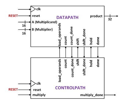
Figure 13. FSM-D Model for BCD Multiplier Architecture.
State transitions of the controlpath were analyzed by following the desired sequence from the operation of the datapath design. A state diagram for the controlpath was then constructed as shown in Figure 14.
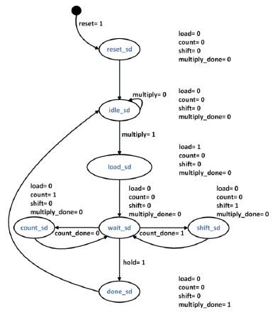
Figure 14. State Diagram for Controlpath of BCD Multiplier Architecture.
3. Hardware Implementation of the 4-Digit BCD Multiplier
The 4-Digit BCD Multiplier system was implemented entirely in VHDL using the Xilinx ISE 14.7 (Pawlak et al., 1997). Sub-modules were port-mapped and interconnected to create the datapath, following the principles and techniques described in (IEEE, 1993) and (Perry, 1998). Finite State Machines (FSMs) were employed to handle the sequencing of the system, drawing knowledge gained from the aforementioned references. Both the datapaths and controlpaths were then integrated by port-mapping them together to create the main system.
4.System Testing
The 4-digit multiplier system was validated by subjecting it to a diverse range of input values, and the actual outputs were compared against the expected results, as presented in Table 1. The validation process involved simulating the system using ISim in Xilinx 14.7 ISE. The results shown in Table 1 demonstrate that the multiplier system accurately computes the product of the inserted inputs. Table 2 depicts FPGA platforms used in verification testing.
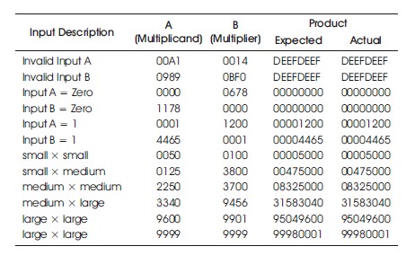
Table1. Verification Test Results.
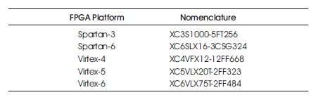
Table2. FPGA Platforms used in Verification Testing.
The maximum path delay of the overall 4-digit BCD Multiplier system with and without similarity investigation was obtained for several FPGA targets using available Post Place and Route Static Timing Reports as depicted in Table 3.
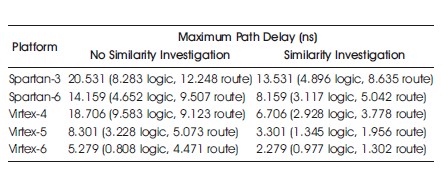
Table 3. Maximum Path Delay with Similarity Investigation.
Table 4 gives the comparison of the maximum path delay of the 4-digit BCD Multiplier system and existing multiplier systems.
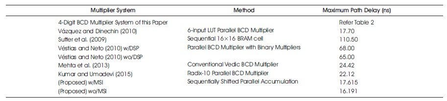
Table 4. Comparative Analysis of BCD Multiplier Core
5. Discussions
It was discovered that the inclusion of the Similarity Investigator in the 4-digit BCD multiplier core resulted in a significant reduction in path delay. Compared to the multiplier system without similarity investigation, the version with similarity investigation exhibited a shorter maximum path delay across all tested platforms. This improvement becomes increasingly crucial as the number of unique multiplier operations grows over time. The hardware utilization on the Spartan-3 with and without Similarity Investigation is given in Tables 5 and 6. As more multiplier operations are performed, the utilization of the RAM blocks is expected to increase. However, it is important to note that there is a limit to the number of unique multiplications that can be carried out before the system experiences diminishing returns. The hardware utilization on the Spartan-6 with and without Similarity Investigation is given in Tables 7 and 8. In the case of the multiplier reported in this paper, a total of 879 unique multiplications can be performed before reaching this point. Therefore, optimizing the path delay of the similarity investigator becomes paramount as more multiplier operations are executed. The hardware utilization on the Virtex-4 with and without Similarity Investigation is given in Tables 9 and 10.
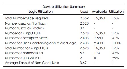
Table 5. Hardware Utilization on the Spartan-3 with Similarity Investigation.
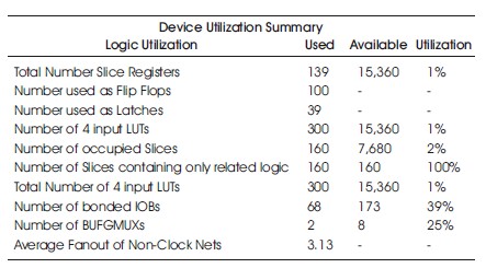
Table 6. Hardware Utilization on the Spartan-3 without Similarity Investigation.
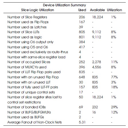
Table 7. Hardware Utilization on the Spartan-6 with Similarity Investigation.
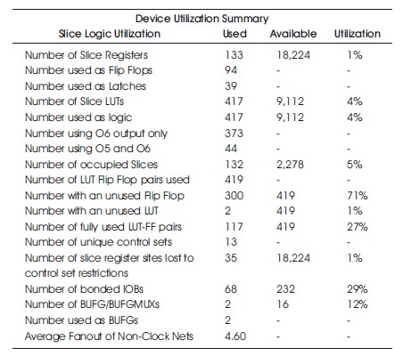
Table 8. Hardware Utilization on the Spartan-6 without Similarity Investigation.
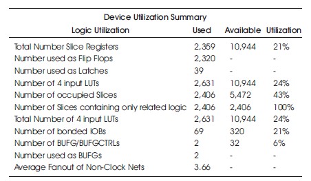
Table 9. Hardware Utilization on the Virtex-4 with Similarity Investigation.
Table 10. Hardware Utilization on the Virtex-4 without Similarity Investigation.
The 4-digit BCD multiplier demonstrates superior path delay performance compared to existing reviewed multipliers. Its path delay is at least 23% lower than the BCD multipliers (Sutter et al., 2009; Vázquez & Dinechin, 2010). This achievement is attributed to the chosen parallel multiplication approach, which eliminates the partial product reduction stage. Additionally, preserving arithmetic in BCD format plays a critical role in avoiding the need for BCD-to-binary and binary-to-BCD conversion operations, which would negatively impact both the maximum path delay and hardware utilization of the 4- digit BCD multiplier. The hardware utilization on the Virtex-5 with and without Similarity Investigation is given in Tables 11 and 12. The multiplication algorithm employed in this study capitalizes on the place value of base-10 decimal numbers. This approach reduces multiplication to a series of accumulations of sequentially shifted digits, further contributing to the efficient performance of the system. Moreover, the validator component of the multiplier effectively handles invalid BCD inputs, multiplications by one, and multiplications by zero. This successful handling of exceptional cases prevents erroneous computations and significantly reduces the path delay in the multiplication process. The hardware utilization on the Virtex-6 with and without Similarity Investigation is given in Tables 13 and 14.
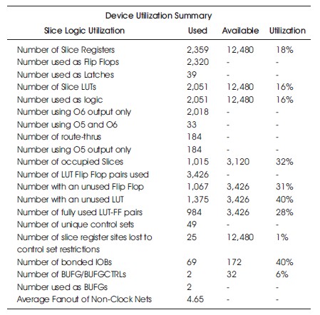
Table 11. Hardware Utilization on the Virtex-5 with Similarity Investigation.
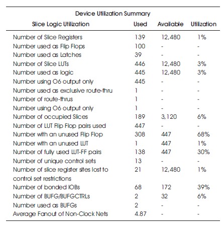
Table 12. Hardware Utilization on the Virtex-5 without Similarity Investigation.
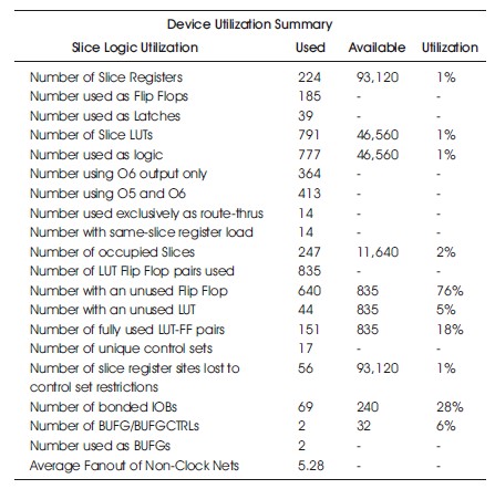
Table 13. Hardware Utilization on the Virtex-6 with Similarity Investigation.
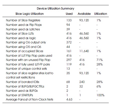
Table 14. Hardware Utilization on the Virtex-6 without Similarity Investigation.
Conclusion
A 4-digit BCD multiplier core was successfully designed and implemented on the Spartan-6 XC6LX16-CS324 FPGA using the Digilent Nexys3 toolkit and the Xilinx ISE 14.7 software. The integration of similarity investigation into the multiplier system resulted in a notable reduction of the maximum path delay. The designed multiplier core has the capability to detect invalid BCD inputs and promptly issue an error warning. It also incorporates an optimization strategy to avoid performing lengthy multiplication operations when either of the inputs is equal to one or zero, providing a trivial result instead. These features contribute to the overall efficiency and reliability of the multiplier system. However, it is important to acknowledge that as the number of unique multiplier operations increases, the multiplier system may encounter diminishing returns. To address this, upgrading the RAM blocks to enhance data accessibility is a viable approach. Additionally, further upgrades should be pursued to optimize the path delay and improve hardware utilization of the multiplier system. By focusing on these areas of improvement, the 4-digit BCD multiplier core can be enhanced to meet the evolving needs and demands of multiplication operations, ensuring its continued effectiveness and efficiency.