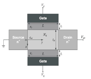
Figure1. The Schematics of a Junction Less Double Gate MOSFET
Semiconductor junctions are present in all existing transistors, and transistors are the fundamental building blocks of modern electronic devices. A strongly doped device with the same type of doping in the channel area as the source and drain regions is known as a junction Less (JL) transistor. Chipmakers utilise junction-less transistors to build smaller devices. This work examines junction Less Double Gate (JL DG) MOSFETs with Threshold Voltage Roll-Off (TVR), DIBL, and Sub-threshold Swing
Transistors are the fundamental components of modern electrical devices. Junctions are present in all transistors. The most common type of junction created by contact between P-type and n-type semiconductors is the PN junction. The metal oxide semiconductor field effect transistor (MOSFET) is made up of two PN junctions. Integrated Circuits (IC) frequently use this type of transistor. However, as technology has progressed, traditional junction-based MOSFETs have faced numerous obstacles and constraints, such as Short Channel Effects (SCE). As a result, junction-less (JL) transistors were used, which had homogeneous doping concentration in the source, drain, and channel regions. JL devices overcome process constraints such as wide doping concentration gradients and limited thermal budgets due to their junction-free nature (Chiang, 2012). JL transistors (JLT) provides various advantages due to the lack of junctions, including easier fabrication without a deep source or drain implants, extremely low short channel effects, extremely low leakage current with virtually optimum sub-threshold slope, and optimal gate control over the channel potential(Sarma & Sharma, 2015.
Unlike a junction-based transistor operating in the surface conduction mode, the inherent behavior of JL MOSFETs operating in the volume conduction mode substantially reduces surface roughness dispersion and increases carrier transit speed. Because of the high doping in the channel region, the JL transistor has a disadvantage in that it reduces carrier mobility (Chiang, 2012). Many innovative device architectures and channel materials, such as multi-gate MOSFETs, have been proposed to solve these limitations. A new MOSFET construction known as the Double Gate (DG) MOSFET has been proposed. Since the back gate can effectively block out the field presentation from the drain and hence prevent the short channel effects (SCE), DG MOSFETs can be scaled to the smallest channel length achievable for a given gate oxide thickness. The front and back gates of a DG MOSFET can be controlled jointly to increase the ION/IOFF ratio.
The model, in addition to providing a physical understanding of device physics, provides basic design guidelines for JL double-gate MOSFETs and may be simply applied to the analysis of threshold voltage behaviour due to its simple formula and computational efficiency.
The N+ -N+ -N+ structure of a junction Less Double Gate (JL DG) Transistor has consistent doping concentration for the source, channel, and drain, as shown in Figure 1. L, tsi, tf and tb are the gate length, channel thickness, front gate oxide thickness, and back gate oxide thickness, respectively. The JL DG structure in our suggested model is symmetrical.
We offer an analytical model for surface potential using 2D Poisson's equation in this study. The ATLAS TCAD device simulator is used to verify the accuracy of our suggested model. We also looked at how sub-threshold swing, drain induced barrier lowering, and threshold voltage roll-off changed as channel length increased. The result demonstrates that the JL DG gadget is highly resistant to short channel effects
Figure1. The Schematics of a Junction Less Double Gate MOSFET
JL transistors operate on a completely different principle than standard MOSFETs. In contrast to conventional MOSFETs, which induce minority carriers at the semiconductor& ndash; insulator interface, the JL MOSFET's gate bias depletes or accumulates majority carriers from the heavily doped silicon substrate. The growing gate voltage will conduct the channel that has been pinched off by the flat-band voltage caused by the work-function difference between the gate electrode and silicon layer in a normally off JL MOSFET. The JL MOSFET's majority carriers effectively flow in the volume of the silicon film, as opposed to the conventional MOSFET's minority carriers, which flow at the surface between the silicon film and gate oxide
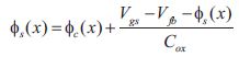
Figure 1 depicts the standard device structure for JL double-gate MOSFETs, which has been used to create the model. The channel area can be assumed to be totally depleted in the sub-threshold operation domain, and the 2D Poisson equation for the n-channel JL double-gate MOSFET can be stated as,
where f(x, y) is the 2D channel potential and Nd is the assumed uniform channel doping density for simplicity. The 2D Poisson equation in Equation (1) can be further simplified to the quasi-2D scaling equation with the bulk conduction mode by making the following assumptions Chiang, 2005).
It yields,
where f (x,y=0) is the central potential, Φc is the long channel central potential, and l is the scaling length. The derivations of Φc and λ are given as,
By inserting Equation (3) and (4) into Equation (1) and eliminating the surface potential, the generalized scaling equation with the bulk conduction mode can be obtained as
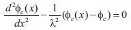
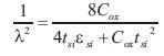
where, the scaling length of λ and central potential of Φc have been shown in Equation (6) and (7) respectively

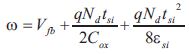
where, Vfb is the flat-band voltage at the silicon film to gate dielectric interface and Cox is the gate oxide capacitance per unit area. The general solution of the ordinary differential equation in Equation (2) can be obtained as,
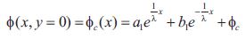
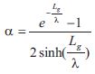
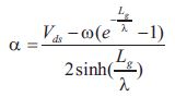
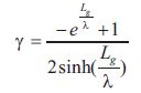
With the boundary condition of Φ(x=0, y=0)=0 and Φ(x= Lg , y=0)= Vds, a and b in Equation (6) can be obtained as,


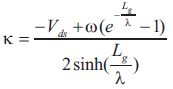
By solving gate bias Vgs, obtain the short-channel threshold voltage for JL double-gate MOSFETs
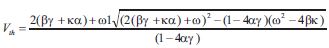
The coefficients of a and b in Equations (12) and (13) approach zero for the long-channel device, and Equation (16) will be decreased to ω, which is the same as the threshold voltage for the long-channel JL double-gate MOSFETs Duarte et al.,2011;Rios et al., 2011. It should be noted that for a generally off long-channel device, w can be a positive value and for a normally on long-channel device, it can be a negative value.
The 2D device simulator DESSIS (Device Simulation for Smart Integrated Systems) is utilized to test the suggested model (Weis et al., 2008). The threshold voltage roll-off vs. effective channel length for various silicon-film thicknesses is plotted in Figure 2. Comparisons are conducted between the Junction-less Dual Metal (JLDM) MOSFET simulation results and the JBIM MOSFET simulation results. The threshold voltage roll-off will be aided by the shorter effective channel length, as can be seen in Figure 2. The thin silicon film of tsi = 5 nm would effectively alleviate the threshold voltage roll-off when compared to the thick silicon film of tsi= 15 nm, especially when the effective channel length is further lowered to 10 nm.
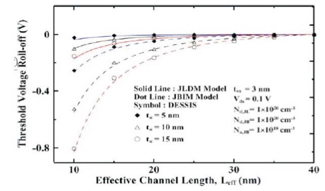
Figure 2. Threshold Voltage Roll-Off Versus Effective Channel Length
The JBIM device will experience more SCEs and produce more threshold voltage degradation than the JLDM device due to source/drain intrusion on the channel area. Although the thin silicon film is essential to prevent SCEs and limit threshold voltage roll-off, it reduces the JLDM/JBIM transistor's current driving capabilities.
Comparisons are made between the JLDM device's simulation findings and those of the JBIM device. For the silicon film of the JLDM device and the source/drain area of the JBIM device, high N-type doping densities of Nd,JL=1×10⁻³ cm and Nd,JB = 1×1020 cm are utilized, respectively. The silicon film of the JBIM device has a P-type doping density of Na,JB =1×1018 cm-3. Lg is the effective channel length for the JL device, and Lg -Ls -Ld +2LD is the effective channel length for the JB device Dhiman & Ghosh, 2017;Granzner et al., 2007;Trivedi & Fossum, 2005
The DIBL is defined as the difference between the low drain bias threshold value of Vds1 = 0.1 V and the high drain bias threshold voltages of Vds2 = 0.5, 1.0, and 1.5 V. When the device is shrunk into the deep sub-micrometer regime, the growing drain bias will cause severe DIBL. A modest drain bias is required to properly suppress DIBL. Again, the JBIM device has greater DIBL than the JLDM device due to source/drain encroachment on the channel region.
In Figure 3, the DIBL fluctuation with effective channel length for various drain biases is presented, and the JLDM MOSFET simulation results are compared to the JBIM MOSFET simulation results
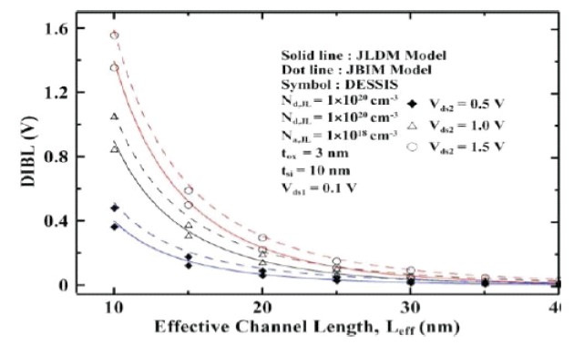
Figure 3. DIBL Versus Effective Channel Length
It is possible to refer to the analytical model of the sub-threshold swing. The JLAM/JBIM device has the smallest/largest sub-threshold swing due to the best/worst short-channel behaviour among the JLDM, JLAM, and JBIM devices. Although Quantum Mechanics Effects (QMEs) are not taken into account in this study, it has been discovered that QMEs increase the channel potential barrier and threshold voltage when compared to classical electrostatic effects.
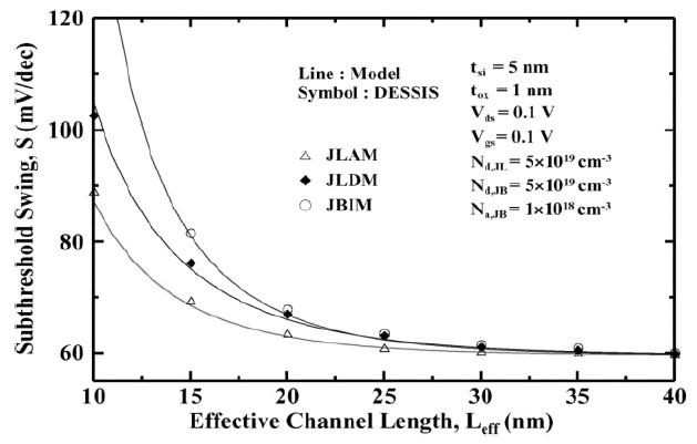
Figure 4. Sub-Threshold Swing Versus Effective Channel Length
For the JLDM, JLAM, and JBIM devices, Figure 4 depicts the fluctuation of sub-threshold swing with effective channel length. For the silicon film of the JLAM/JLDM device and the source/drain area of the JBIM device, high N-type doping densities of Nd,JL = 5x1019 cm3 and Nd,JL=5x1019 cm3 are employed. The silicon sheet of the JBIM device has a P-type18 3 doping density of Na,JB =1x1018cm3.
A short-channel threshold voltage for JL double-gate MOSFETs has been constructed using the bulk conduction mode of the quasi-2D scaling equation. The model can also be used to mimic the JL/JB device's AM/IV functioning mode. The JL device outperformed the JB device in terms fully of threshold roll-off reduction, DIBL reduction, sub-threshold swing reduction, and design space expansion. When the channel length is shortened in the JL/JB device, both thin silicon film and thin gate oxide are required to prevent the threshold voltage roll-off. The model, in addition to providing a physical insight into device physics, also gives basic designing assistance for the JL double-gate MOSFET and, because of its simple formula and computational efficiency, may be simply applied to device simulation