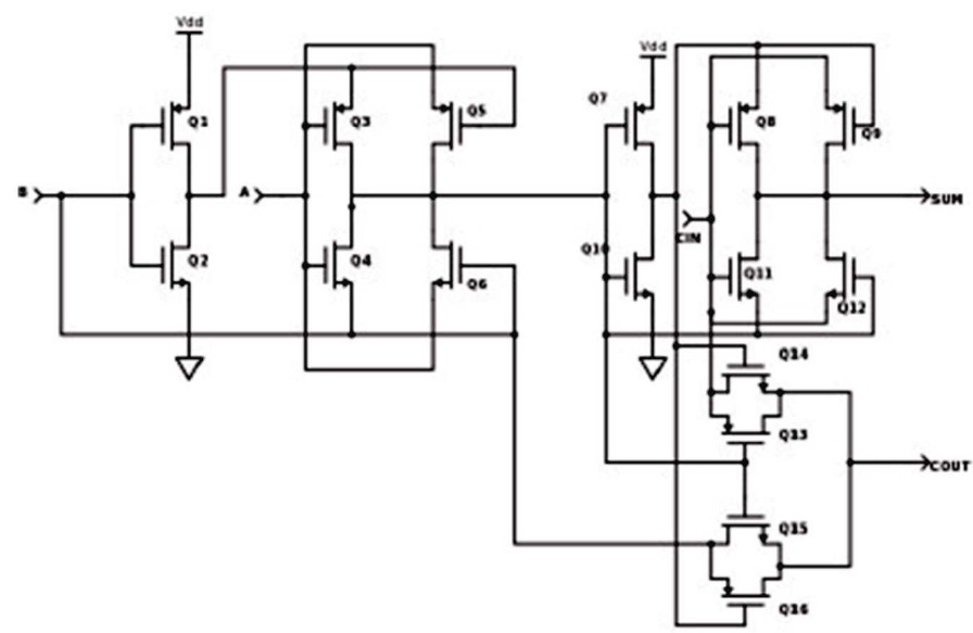
Figure 1. The conventional Full Adder Circuit using Transistor
In recent trends, power optimization and improvement of speed are the key researches in the VLSI circuit design. This paper presents an advanced hybrid full adder. Most of the adder has a powerful impact on the overall performance of the system. The modern design is correlated with some actual designs to enhance performance parameters such as power utilization, delay, and PDP. In the proposed circuit, the power delay product is maximum of 96.8% with respect to Complementary Metal-Oxide Semiconductor (CMOS) at minor frequency. The power utilization is increased at a slow rate in contrast to other adders with increase in frequency. The simulations are drifting out on Cadence Virtuoso at 130 nm. By correlating with the previous Full Adder (FA) designs, the present operation was found to offer a powerful improvement in terms of speed and power.
As the technology advances day by day the demand for low power and high speed operating devices is increasing. Power consumption can be reduced by two factors, by surmounting the supply voltage and changing the operating frequency. But, these factors may increase the propagation delay of the system and driving capability may be reduced. Full adders are the fundamental block of any digital circuit. Thereby, increasing the efficiency of full adders, increases the performance of overall system. VLSI devices contain thousands of gates within a single package. Large memory arrays and complex microcomputer chips come under VLSI. CMOS technologies combine both Ptype Metal-Oxide-Semiconductor (PMOS) and N-type Metal-Oxide-Semiconductor (NMOS) transistor (Rabaey, Chandrakasan, & Nikolic, 2002) devices on the same silicon. Both the transistors require two different substrates, that is NMOS transistor requires a p- substrate and the PMOS transistor requires an n-type substrate. Every electronic circuit requires a certain amount of power to operate. The power dissipation is a parameter that is measured in milliwatts (mW). It represents the losses associated with the device that are usually dissipated as heat. The sum of the entire power dissipated by all gates, circuits or IC's in the design is considered as the power consumed by the system. Propagation delay is the most important factor to measure the performance of the circuit. Time taken to propagate a signal from the input of the gate to the output of the gate is called the propagation setback of the gate.
The main motto of this paper is to develop a modernized Hybrid Full Adder (HFA) to reduce the power and improve the speed, overall performance of the system with the aid of the special function gates (EX-NOR,EX-OR). By using these gates the internal carry bit generating time period i.e., Propagation delay for the next level of the full adder input is minimized. The significance of the proposed work is that it increases the transistor performance and it reduces the power rails in between the sink and source nodes. The suggested work is to offer a dynamic improvement in the speed and power, as well as improve the efficiency of the system.
Many of the previous researchers have concentrated on power utilization, speed improvement and efficiency of the system. In general there are three constituting modules for full adder design (Zimmermann & Fichtner, 1997). The authors have presented the performance analysis of low power 1-bit CMOS full adder cells. By combining the different modules, there are twenty different full adder designs are implemented. Each design has several advantages in itself like power consumptions, speed, area, delay, and device count. The low-voltage low-power CMOS full adder are discussed by many authors (Vesterbacka,1999; Radhakrishnan, 2001). In general, the designed circuits have used the kmaps and pass network theorems and six-transistor XORXNOR cell is implemented with the aid of standard rules. The standard method has no effect on voltage drop in transistors (Radhakrishnan, 2001). It does not affect the threshold voltage drop in MOS transistors, but at the same time, fewer transistors are used compared to existing designs. However, more design effort is required for the sizing of the transistors explained and to design the vigorous, energy-efficient 1-bit full adders for deep sub micrometer design using hybrid-CMOS logic style (Shams, Darwish, & Bayoumi, 2002). Novel 1-bit full adder using hybrid logic is presented here for low Power consumptions. Proposed design is performed with low power voltage levels. Low-power high- speed CMOS full adders are core for embedded systems (Sudsakorn, Tooprakai, & Dejhan, 2012; Goel, Elgamel, & Bayoumi, 2003). Generally, the power utilization and high speed are considered as the main factor for the adequate design (Goel, Kumar, & Bayoumi, 2006; Chang, GU, & Zhang, 2005). The driving capability, can be improved with low power by using a new exclusive OR gates the full adder is integrated in a System on Chip (SoC) (Tung, Hung, Shieh, & Huang, 2007; Aranda, Báez, & Diaz, 2010; Wairya, Singh, Nagaria, & Tiwari, 2011). Many of the designed circuits are facing power dissipation due to leakage currents of the whole static and dynamic cases and its analysis (Deb & Majumder, 2016; Pattnaik et al., 2017). Shin and Kim (2004) presented the minimization of the leakage power under certain circuit timing constraints. The special function gates have to satisfy the universal and basic gates principles, to reduce the component count.
Most of the research work have been done on the power dissipation and delay in 1-bit full adder design, developed with aid of NAND and NOR gates. The simulation results of the corresponding designs having the power dissipation and delay values are 0.2040 mW, 65.0371ns respectively. Similarly, the transistor component counts are also high in the existed works, to avoid the problems in the earlier research the author mainly focusing on delay, power minimization and improves the efficacy of the system.
In conventional methods, an Adder is designed by using transistors. The Chang adder design is performed with 16 transistors and its modified low power XOR and XNOR circuit is shown in Figure 1. An addition of more transistors solves the delay problem, but these designs leads to the higher power utilizations. Aguirre adder is performed with parallel pass transistor logic style to find the balanced paths based on multiplexing of the Boolean functions. Full swing balance output is generated by the Goel adder with XOR- XNOR circuit. These circuit are used for the high speed applications because of its cross coupling. Complementary pass transistor logic is evaluated by the Agarwal adders to determine the full fluctuation output voltage. This hybrid adder has a generation of SUM and CARRY OUT signals. Truth table for 1-bit full adder has been mentioned in Table 1. 1-bit Full Adder Transistor sizes are mentioned in Table 2.
Figure 1. The conventional Full Adder Circuit using Transistor
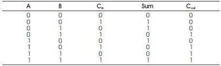
Table 1. Truth Table of 1-Bit Full Adder
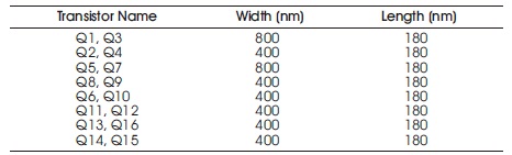
Table 2. Transistor Sizes of Proposed 1-Bit Full Adder
The hybrid logic design style involves the division of larger circuit into smaller sub-circuits and each sub circuit is optimized using various logic design style. The hybrid design methodology for a full adder circuit is shown in Figure 2. The Figure 2 shows that the full adder circuit is split into 3 sections and these sections are designed using different design styles to exploit the advantages of the different design styles and essence the desired performance. Module 1 produces XNOR and XOR behavior of the inputs A and B. The module1 can be either XNOR based or XOR based depending on the primary output generated within the module. The primary output is utilized to get the other output using an inverter. Module 2 and Module 3 comprises of the circuitry to produce the required sum and carry outputs of the full adder by appropriating the intermediate outputs achieved by module1 circuit.
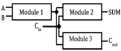
Figure 2. Schematic Diagram of Hybrid Full Adder
XNOR module consumes more power in the proposed adder design. Power can be reduced to a desirable extent by optimizing the XNOR module. It also wards off the possibility of voltage degradation.
The schematic of this module is given in Figure 3. The transistors Mp7, Mn7, Mp8 and Mn8 are implemented in order to get the required carry out signal. Here input carry signal (Cin) passes or propagates through only one transmission gate, i.e., Mn7 and Mp7. Hence it reduces the path required for carry propagation. Large channel width transistors are used for transmission gates. Here Mn7, Mp7, Mn8 and Mp8 form the transmission gates. Hence it results in reducing the delay for some extent. The Figure 4 and Figure 5 represents the simulation results of the 1-bit hybrid full adder and 4-bit ripple carry adder. Here x-axis shows the time and y-axis the voltage level of the input and output signals. Here the voltage levels are varying from 0 V to 5 V. The Table 3 shows the proposed design’s power dissipation and delay values.
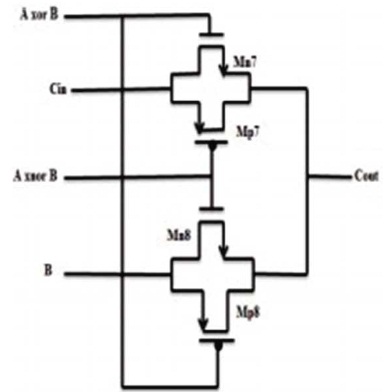
Figure 3. Carry Generation Module
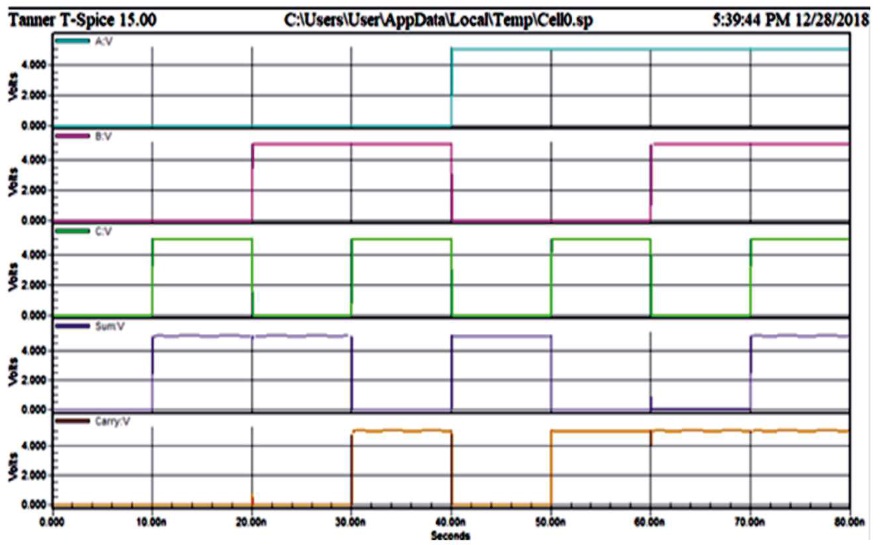
Figure 4. Waveforms of Full Adder
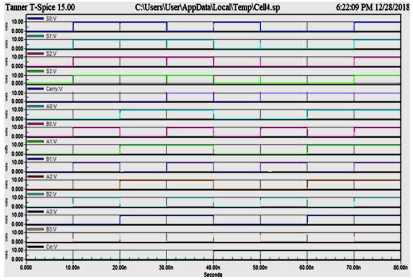
Figure 5. Waveforms of Ripple Carry Adder
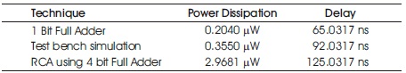
Table 3. Power Dissipation and Delay Comparison
Numerous full adder circuits can be cascaded in coordinating to add an N-bit number. For an N- bit parallel adder, there must be N number of full adder circuits. A ripple carry adder is a logic circuit, in which the carry-out of each full adder is the carry in of the consecutive next most significant full adder. Each carry bit gets rippled into the next stage that is simply called as ripple carry adder. In Half adder sum and carry out bits in the ripple carry adder is not accurate until the carry in of that stage appears. The reason behind this is propagation the delays that existed inside the logic circuit is the time required between the input and corresponding generated output. The inverter gate principle is, for the given input “0” it produce the output as “1” and vice versa. The propagation delay in the inverter gate or any gate is decided by changing the states transition period. Similarly, the carry propagation delay is the time taken for the corresponding carry-in to the occurrence of the carry-out value. Circuit diagram of a 4-bit ripple carry adder is shown in Figure 6. The block diagram of Ripple carry adder using Hybrid Full adder is shown in Figure 7.
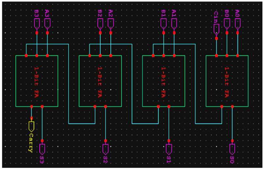
Figure 6. Schematic Representation of 4-bit Ripple Carry Adder

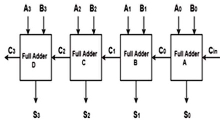
Figure 7. Ripple Carry Adder using Hybrid Full Adder
The proposed designs of 1-bit full adder circuit with CMOS technology have been simulated by using Cadence tool.
The 4-bit RCA is having 4 bits of data from A0-A3 and similarly data B0-B3. In adder circuit initial carry bit Cin = 0, here the internal carry generating time for the next level of the adder input value is reduced. The simulation results are verified using the Cadence tool.
The main aim of this paper is minimizing the power and delay time between the input and output. The Figures 4 and 5 discuss the clear picture of the proposed work. A single bit hybrid full adder have the inputs A, B, and C and generates sum (S), carry (C) as outputs if any one of the input are high then only sum will be high (1) otherwise sum = 0 whereas in the carry generator if any two or three inputs are high then we get carry bit (Cout = 1). The voltage level are varying from 0V (min) to 4V (max) and scale on Xaxis shows a delay is 10 ns for each unit. Similarly, the Figure 5 represents the 4 bit hybrid ripple carry adder with inputs A0-A3 and B0-B3 and generated outputs are S0-S3 and carry out (Cout). The operation principle is same as the basic adder but it can reduce the internal carry time to nano sec, the corresponding results are mentioned in the Table 3.
Low-power hybrid 4-bit full adder has been proposed to improve the power, delay, speed and efficiency of the system. The simulation is tested and verified with 130 nm Cadence tool. The Table 3 presents the comparison of the power dissipation and delay with respect to the 1-bit and 4-bit RCA. The simulation results are investigated to find out the superiority of the submitted design over the existing designs. In analogy with the actual full adder designs, the modern implementation was found to offer compelling development in terms of speed and power. The suggested work is to promote the transistor performance. It also wards off the possibility of voltage degradation.
Detecting the power and setback time in the VLSI designs becomes the challenging issue. To overcome those issues the proposed idea is one of the best techniques while compared with the other existing works. Based on these inputs the superior hybrid full adder can be developed with the help of LECTOR and Junction less transistors. The suggested techniques are the best methods to improve the performance by minimizing the power consumption and delay.