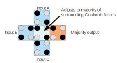
Figure 1. Majority Gate
As a substitute for CMOS, innovation of quantum cellular automata was anticipated by Lent et al, to represent exemplary cell automata with quantum dots. Quantum Cellular Automata (QCA) may be a progressive innovation that endeavors the certain nano level issues to perform computing. Its potential advantages are high speed, high device density, and low power dissipation. This paper presents the design of XOR gate with the least number of cells; furthermore the circuit appearance is simple. Exploitation of this novel XOR gate leads to the development of combinational circuits like Half Adder, Full Adder, Parity Generator and Parity Checker etc., which were developed effectively in a single layer structure with less number of cells, area and delay, as compared to the earlier designs. This paper mainly focusses on the construction of optimized combinational circuits without using cross- overs in QCA. Further, the simulation results are presented.
Due to scaling of technology to accommodate more devices, there are many limitations in shrinking of CMOS (Y.Taur,2002; Shekhar Borkar,1999) . To overcome the above, emerging Nano device QCA was introduced by Lent (P. Douglas Tougaw & Craig S. Lent, 1994). QCA has Nano size and is simple to implement and it is a promising technology at Nano scale for computing. Even though all digital circuits are implemented using CMOS technology, QCA has many advantages over CMOS. In the near future QCA can replace CMOS. QCA has less power dissipation because no current flow takes place between the cells, whereas in CMOS current transfer takes place between the transistors and hence power dissipation takes place.
Due to shrinkage in cell size internal routing becomes complex, still a size in CMOS cannot be reduced due to several factors; with impact on the structure. Where as in QCA the size is simple and even routing can be done by means of the wire propagation like coplanar and multilayer crossovers. Unlike CMOS, in QCA the transmission media and logic elements are present in the same block. In CMOS, only two stages of clock occur i.e., high to low and low to high, whereas in QCA, to avoid coherence four phase clocking has been developed. In CMOS power is taken from external supply only, whereas in QCA supply is taken from the clock itself. In this paper, optimized design of XOR is presented and compared with the existing designs. The applications of XOR like Half Adder, Full Adder, Parity Generator and Parity Checker have been designed with less number of cells, area and delay; as compared with the existing designs.
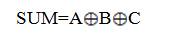
Quantum-dot Cellular Automata is also known as Quantum Cellular Automata (QCA). QCA is implemented by quadratic cells, so they are called QCA cells(K.Kim, K.Wu, R. Karri, 2005). The basic logic primitive gates available in QCA are majority gate and inverter, in which the majority gate contains five QCA cells as shown in Figure 1 to produce the output as logic '1'; if a majority of logic '1' is applied at inputs, else the output is logic '0'.
The inverter or NOT gate can be constructed in two different ways as shown in Figure 2.
Figure 1. Majority Gate
Figure 2. QCA Inverters
AND, OR gates were constructed by polarizing one of the inputs in majority gate of logic '0' and logic '1' respectively (Prameela Kumari N, K.S.Gurumurthy, 2014).
QCA has four phases in clocking (Rumi Zhang, KonradWalus, WeiWang, & Graham A. Jullien,2004).They are switch, hold, release and relax. In switch phase tunneling barriers start to rise. In hold phase the tunneling reaches high to prevent electrons from tunneling. In release phase the tunneling barriers start to lower and in relax phase electrons start to tunnel again.
During the past decade, many combinational circuits were proposed and constructed using QCA (J. Iqbal, F. A. Khanday, N. A. Shah, 2013). The key element in combinational gates is XOR which has wide applications in arithmetic circuits and also in digital communications. XOR gate generates output as logic '1' if the number of inputs is odd or else the output is logic '0'. This key functionality of XOR is useful in many applications such as Half Adder, Full Adder, Parity Generator and Checker. Basic gates AND, OR, NOT and universal gates NAND, NOR can be implemented using a majority gate. Other useful gates XOR and XNOR cannot be obtained directly and its fabrication is also complex. It can be implemented using a combination of basic gates. The gate XOR is implemented using the basic gates AND, OR and INVERTER.
The existing XOR gate design follows the conventional methods by using Demorgans law. The first conventional design of XOR gate is implemented using (1). Initially implemented conventional designs of XOR gate make use of many cells, areas and crossovers. The layout of XOR can be obtained by using different logic functions of basic gates and universal gates. The alternate ways of representing the basic logic function of XOR gate are given below.


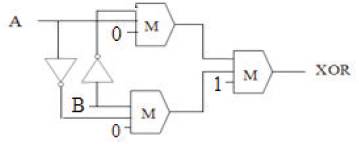
Figure 3. XOR Using Majority Gates
The conventional design of XOR gate in (1) is implemented using majority gates as shown in Figure 3.
This XOR design has a delay of 1 ¼ clock cycle, area 0.08μm^2 and the cell count is 51. Half Adder and Full Adder designs using the above existing design are presented below.
Half Adder has two inputs and it gives two outputs as sum and carry. Half Adder can be obtained by using XOR gate because the sum of Half Adder is equal to XOR output. To obtain carry it requires additional one majority gate compared with the XOR design . The logic implementation of Half Adder is shown below. SUM=A B, CARRY=AB. The design of Half Adder is shown in Figure 4. It has four majority gates and two inverters. This Half Adder design has a delay of 1 ¼ clock cycle, area 0.10μm^2 and the cell count is 64.
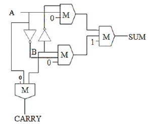
Figure 4. Half Adder
Full Adder can be obtained by cascading two Half Adders. It has three inputs and gives two outputs: sum and carry. The logic implementation of Full Adder is shown in equations (6) and (7).
The existing Full Adder is obtained by cascading the above designed Half Adders; carry of Full Adder is obtained by adding one more majority gate in addition to the half adder circuit. The existing design of Full Adder is shown in Figure 5. It has 9 majority gates and 4 inverters. This Full Adder design has a delay of 2 ¼ clock cycles, area 0.24μm^2, and cell count 150. The comparison of existing full adders constructed with basic gates (Mariam.Momenzadeh, Jing Huang, Mehdi B.Tahoori & Fabrizio Lombardi,(2005), Kyosun Kim, Kaijie Wu, and Ramesh Karri,(2007)) are given in Table 2.
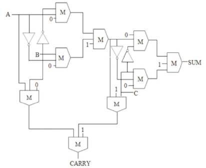
Figure 5. Full Adder
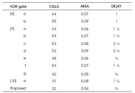
Table 1. Comparison Results of XOR Gate
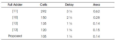
Table 2. Comparison Results of Full Adder
The existing Parity generator & checker was constructed by optimally designed xor gate presented in (M. Mustafa, M R Beigh,(2013)), but it occupies more area and latency as compared with the proposed design.
In any computing system, Adder and XOR gate is the key element in arithmetic circuits. In this paper, the proposed XOR gate was used to construct the optimized Half Adder and Full Adder. The proposed XOR gate design approach follows the conventional methods by using Demorgan’s laws, but construction approach utilizes only three input majority gates and one inverter in an efficient manner to achieve lesser cell count and area. The basic logic function of XOR gate is as follows AB = AB+AB. In order to implement this without any modifications, it needs crossovers. To construct an XOR gate without crossovers, the above expression can be re-written in many ways as in (Mohammad Rafiq Beigh, Mohammad Mustafa, Firdous Ahmad,2013) .
The proposed layout of XOR gate was constructed using (5) which requires less number of inverters as compared to the existing design. Even though this type of XOR gate is constructed using (5), in this design the position of cells is altered thereby it leads to lesser number of cells. By means of using proposed design many circuits can be implemented in single layer itself. In this paper, all designs are constructed by using two cell inverters. Various existing XOR gate design methods are available to construct the QCA with less number of cells and crossovers (Mohammad Rafiq Beigh, Mohammad Mustafa, Firdous Ahmad, 2013). This paper presents the comparison of all existing designs of XOR gate by various methods. Among the existing designs, the proposed XOR gate construction has lesser cell count and latency with no crossovers. Schematic diagram of the proposed XOR gate is shown in Figure 6. The layout and simulation results of the XOR gate are given in Figure 7 and Figure 8 respectively.
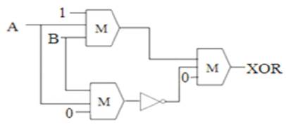
Figure 6. Proposed Design of XOR gate
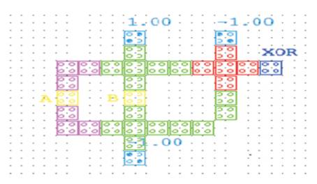
Figure 7. Layout of XOR gate
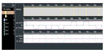
Figure 8. Simulation Results Of XOR gate
The comparison of various existing XOR gate designs with proposed design is shown in Table 1 comparing area,delay and cell count.
From Table 1, it shows that the proposed layout of XOR gate is efficient in terms of cell count and delay when compared to the existing designs.
In the existing Half Adder (Santanu Santra, Utpal Roy, 2014), the XOR gate was constructed by conventional method and sum was achieved directly from the output of XOR gate, but additional gate is required to produce carry at a cost of multilayer structure. But by using (5) both XOR and Half Adder can be obtained in the same circuit. Therefore the Half Adder in this paper can be implemented with less number of majority gates in a single layer structure. The proposed design occupies less area. It has a delay of ¾ clock cycles, area 0.05μm^2 and a cell count of 32. When comparing this design with the existing design, it has ½ delay lesser, area 0.05μm^2 lesser, cell count 32 cells lesser, so the proposed design becomes the optimized design of Half Adder. The design of Half Adder and its simulation results are shown in Figures 9,10 and 11.
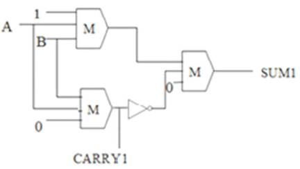
Figure 9. Design of Half Adder
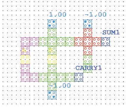
Figure 10. Layout of Half Adder
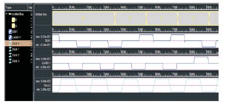
Figure 11. Simulation Results of Half Adder
The proposed Full Adder was optimized by minimizing the carry structure in the existing design (Santanu Santra, Utpal Roy, 2014). The carry path was optimized by using the proposed XOR structured Half Adder and it requires seven majority gates, and two inverters without crossovers. It avoids extra majority gates and crossovers compared with existing design. The proposed design of Full Adder and simulation results are shown in Figures 12, 13 and 14.
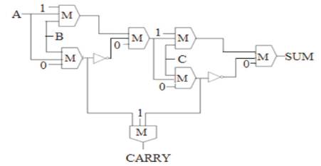
Figure 12. Proposed Design of Full Adder
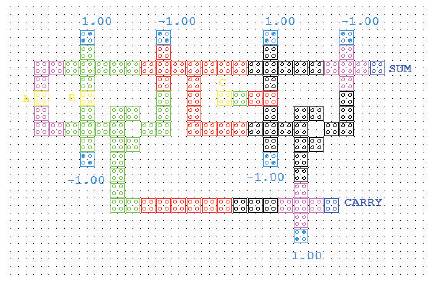
Figure 13. Layout of Full Adder
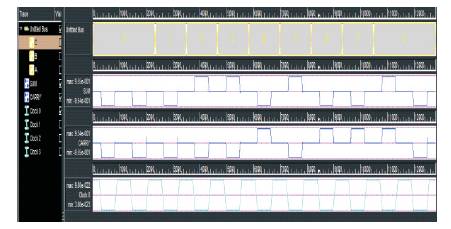
Figure 14. Simulation Results of Full Adder
The comparison results of Full adder with various previous designs are listed in Table 2 in terms of cell count, area and delay. The Full adder in (Heumpil Cho,2006) has a delay of 1 ¼ and is constructed directly to get sum without using XOR, but it has two multilayer crossovers where as in the proposed design, there is no crossover. According to the cost function, the cost of the proposed designs has drastically been reduced by the absence of crossovers (Weiqiang Liu,Liang Lu, M´aire O'Neill, & Earl E.Swartzlander.Jr,2013). Generally cost function proposed by Thomson related to the area and delay is A*Tn , where A is area, and Tn is delay.
There are several applications using XOR design. This paper presents one of the applications of XOR which is Parity Generator and Parity Checker for error detection purpose. In both Parity Generator and Checker XOR plays a major role, which is the basic primitive gate in both circuits.
Parity generator is a combinational circuit used to generate the parity bit, this parity bit is appended along with the data while transmitting data from the transmitter node to the receiver node. Parity generator is of two types. They are odd parity generator and the even parity generator. In even parity, the parity bit is obtained as zero if the number of 1's in the data is even; else it is one. In the same way in odd parity, the parity bit is obtained as zero if the number of 1's in the data is odd else it is one. In this paper, even parity generator has been implemented using optimized XOR design. The logic implementation of parity generator using majority gates is shown in Figure 15, its layout and simulation results are given in Figure 16, and Figure 17.
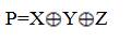
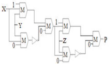
Figure 15. Proposed Design of Parity Generator
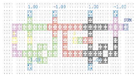
Figure 16. Layout of Parity Generator
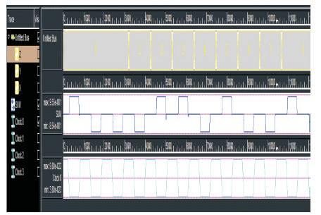
Figure 17. Simulation Results of Parity Generator
At the receiving-end a parity checker is used to detect single bit error in the transmitted data word by regenerating the parity bit in the same fashion as the generator and is then compared with the transmitted parity bit. If the transmitted data has 3 bits message and one bit, even parity is transmitted to their destination. Here a parity checker circuit checks the possible errors in the transmission. Since the message was transmitted with even parity bit, the received four bit message must have an even number of 1's. The logic implementation of parity checker is shown in Figure 18. The layout and simulation results of the proposed parity checker is given in Figure 19 and Figure 20 respectively. All the layouts and simulation results in this paper were obtained by using QCA designer tool (Konrad Walus, Timothy J. Dysart, Graham A. Jullien & R. Arief Budiman,2004).
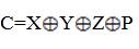
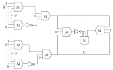
Figure 18. Proposed Design of Parity Checker
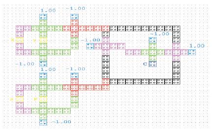
Figure 19. Layout of Parity Checker
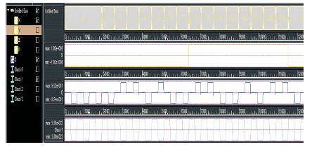
Figure 20. Simulation Results of Parity Checker
This paper presents the design, layout and simulation of Half Adder, Full Adder and error detection circuits such as Parity Generator and Parity Checker based on optimized XOR configuration. The proposed designs were constructed without using cross-overs to reduce the cost function and to improve the layout regularity. Layouts were simulated using QCAD Tool. Table 3 clearly shows that the area and delay of the proposed parity generator has reduced 40% in comparison with earlier design. The proposed parity checker design was improved by a reduction of 30% in area and 60% in delay compared with the existing design as reported in Table 4. Hence the proposed designs are efficient in terms of delay, area and cell count compared with the already existing ones. An attempt is made in this paper to optimize the circuits and to construct the combinational circuits in a single layer structure.
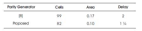
Table 3. Comparison Results of Parity Generator
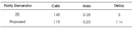
Table 4. Comparison Results of Parity Checker