(1)
FIR filters are basic building blocks in Digital Signal Processing applications, require computationally efficient multiply and accumulate operations so the blocks with the desired characteristics have to be chosen carefully. The multiplier is generally slow and occupies large area, the adder also contributes to long delay when the length of the addition is more. Improving the speed results mostly in large areas, usually they conflict with each other. The signal processing applications consume considerable amount of energy. Hence there is a need for low power, high speed, low area circuits for Digital Signal Processing applications. The aim of this paper is to implement a low power, high speed, area efficient FIR filter. Multiply and Accumulate technique is used for multiplier design and the addition and accumulation operations are performed by Parallel Prefix Adders. Some of the available Parallel Prefix Adder architectures and the hybrid architecture of Parallel prefix adder is used here. The implementation is done for 4- tap FIR filter using Xilinx 14.5 version, with the targeted device of Spartan3E FPGA. The experimental results show that the implemented FIR filter using hybrid parallel prefix adder is efficient in area, consume low power and has high speed compared to existing parallel prefix adder models.
Computers are extremely capable in two broad areas, they are: Data manipulation and Mathematical calculation. Traditional microprocessors are primarily directed at data manipulation. Digital Signal Processors (DSPs) are designed to perform the mathematical calculations needed in Digital Signal Processing (DSP). The DSP market is very large and growing rapidly. This is because of the demand for better and cheaper consumer products, such as: Cellular telephones, multimedia computers and high fidelity music reproduction. The digital filter is a building block and has a number of attractive digital signal processing applications. The computational complexity of a digital filter structure is given by the total number of multipliers and the total number of two-input adders required for its implementation, which roughly provides an indication of its cost of implementation [13,40].
FIR filter is the most common DSP technique. The FPGA based FIR filters using traditional arithmetic requires considerable Multiply-and-ACcumulate (MAC) blocks with the increase in the order of filter. As the performance requirements of these filters started increasing various approaches are proposed in the literature [8,24,48,37]. Field Programmable Gate Arrays (FPGAs) are parallel structures containing a uniform array of Configurable Logic Blocks (CLBs), memory, DSP slices and some other elements. The main advantage of FIR filter in an FPGA is the ability to adopt the implementation to match the system requirements [ 1-2, 4 ,11- 12,38] With the implementation of FIR filters on FPGA, the performance of the filter can be estimated [6,41] .
In literature various multiplier-less schemes have been proposed for FIR filter realization. These methods are of two types, one of the methods is a Canonic Sign Digital (CSD) method, in which the coefficients are represented by a combination of powers of two in such a way that multiplication can be simply implemented with adder/subtractor and shifters [22,47,49]. The second type of multiplier-less method use memory (RAMs,ROMs) or Look-up Tables (LUTs) to store pre-computed values of coefficient operations; this method is called Distributed Arithmetic(DA) method [7,25,32-33,46]. For higher throughput, FIR filters are implemented with parallel and pipeline architectures [9,23,36]. In [8], signed amplitude representation for the coefficients and two's complement for the input samples are used to reduce the hardware requirement. As the coefficients of an FIR filter are constant, the multiplication in FIR filter can be done with Multiple Constant Multiplication (MCM) block. This is a performance bottleneck in many DSP systems, which can be reduced by properly sharing the partial products in MCM blocks [12] and also by eliminating common sub expressions from the representations of the constants [10,13,21,31,42] .
The rest of the paper is organized as follows: In section 1, FIR filter design is given. The implementation of Multiplier block using shift-and-add technique is discussed in section 2. Section 3 describes various parallel prefix adder architectures and their implementation. The design methodology for the implementation of FIR filter is given in section 4. Experimental results are presented in section 5. Conclusions and Future scope are presented in the last section.
FIR filter is the most widely used DSP technique. The N-tap FIR filter is normally described by the following equation [13,40].
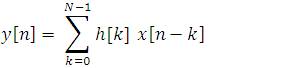
Where N is the number of coefficients (or taps) of the filter, h[n] represents filter coefficients, x[n], y[n] are the input and output sequences respectively. The N-tap FIR filter is characterized by N coefficients and in general, requires N multipliers and (N-1) two-input adders for implementation. Structures in which the multiplier coefficients are the same as the coefficients of the transfer function are called direct-form structures. A direct-form realization of an FIR filter can be readily developed from Eq.(1) as indicated in Figure 1 for N=4.
An analysis of this structure yields

which is precisely of the form of Eq.(1).
The transpose structure is shown in Figure 1. Figure 2, is the second direct-form structure. Both direct-form structures are canonic with respect to delays.
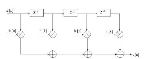
Figure 1. Direct form of FIR structure for N = 4
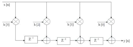
Figure 2. Transposed form of a 4-tap FIR filter implementation
This paper considers the transposed form of architecture of Figure 2 for implementation. This architecture involves multiplying all the coefficients by the same input data. As the registers are in between the adders, the resulting circuit is faster, since the critical path is smaller. This transposed form of FIR filter is best suited for FPGA implementation [13,40]
It is widely accepted that the multiplication is the main source of complexity in an FIR filter. In other words the multiplication consumes most area and is the main source of delay. Additions are the main source of power consumption in the multiplication block.
This paper focuses on the implementation of Multiplier block that increases the speed of multipliers and adders as well as reducing the area and power among the suitable architecture, which is used for Multiplier and Accumulate (MAC) design. The implementation of Multiplier block using Shift-and Add technique is discussed in the next section.
Multiplication schemes are commonly classified into three general types: sequential, parallel and array multipliers. This is not a universal classification and some hybrid multiplication schemes do not fall into exactly any of these categories. Sequential multipliers generate the partial products sequentially and add each newly generated partial product to the previously accumulated sum. The sequential multipliers were popular when the hardware was expensive and bulky. They are still in use in applications where the speed is not critical. Shift and Add multiplication is an example of sequential multiplier [15]. The parallel multipliers generate all partial products in parallel and then use fast multi-operand adders for their accumulation [39]. Array multipliers are essentially regular structures and are similar to expand. In array multiplication, we need to add as many partial products as there are multiplier bits [34]. The Wallace tree multiplier is considerably faster than a simple array multiplier. The Wallace tree's wiring is much less regular and more complicated. As a result, Wallace Trees are often avoided by designers, since design complexity is a concern to them. Wallace tree styles are generally avoided for low power applications [17,34]. Booth multiplier can be used in different modes such as radix-2, radix-4, radix- 8, etc. Modified Booth Encoding (MBE) is most often used to avoid variable size partial product arrays [26,34,39].
In this present paper the multiplication is performed using shift and add technique. Shift-and-add multiplication is similar to the multiplication performed by paper and pencil. To multiply two numbers by paper and pencil, the algorithm is to take the digits of multiplier one at a time from right to left, multiplying the multiplicand by a single digit of the multiplier and placing the intermediate product in the appropriate positions to the left of the earlier results.
In the case of binary multiplication, since the digits are 0 and 1, each step of the multiplication is simple. If the amplification digit is 1, a copy of the multiplicand (1Xmultiplicand) is placed in the proper positions; if the multiplier digit is 0, a number of 0 digits (0Xmultiplicand) are placed in the proper positions. The Circuit of shift-and-add method of multiplication for two n-bit numbers is shown in Figure 3.
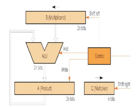
Figure 3. A multiplier Circuit of Shift-and-Add method of multiplication for two n-bit numbers
The 2n-bit product register (A) is initialized to 0. The basic algorithm shifts the multiplicand register (B) left one position each step to align the multiplicand with the sum being accumulated in the product register. The authors use a 2n-bit multiplicand register with the multiplicand placed in the right half of the register and with 0 in the left half.
Figure 4, shows the basic steps needed for the multiplication. The algorithm starts by loading the multiplicand into the B register, loading the multiplier into the Q register, and initializing the A register to 0. The counter N is initialized to n. The least significant bit of the multiplier register (Q0 ) determines whether the multiplicand is added to the product register. The left shift of the multiplicand has the effect of shifting the intermediate products to the left, just as when multiplying by paper and pencil. The right shift of the multiplier prepares the next bit of the multiplier to be examined in the following iteration.
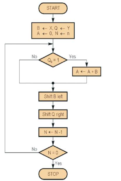
Figure 4. The multiplication algorithm
In the implementation of multiplier block, addition is performed by the parallel prefix adders, because parallel prefix adders are designed for high speed computing, which will speed up the multiplication process also. For shifting operation, barrel shifter is used, by loading it initially with the required value, i.e the upper half with zeros and lower half with multiplicand bits.
The main disadvantage of conventional ripple carry adder structure is longest path delay. The parallel prefix adders are developed for high sped operation of addition operation. Various parallel prefix adders are proposed in the literature of different constraints like area, timing, logic depth, fan-out capability and logic levels of implementation [3,5,14,16,18-20,27- 30,35,43-45].
In every bit(i) of the two operand block, the two input signals (a and b ) are added to the corresponding carry- i i in-signal (carry ) to produce sum output (sum). The i i equation to produce the sum output is
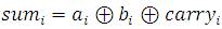
Parallel prefix adder architectures contain tree like structures which compute the required carry input (carry ) i for every bit of addition. The tree structures are developed by using different operators, which receive, generate and propagate signals of previous level and compute, generate and propagate signals for next level [27,30]. The realization of these operators, for enhancement of speed characteristic is also developed [29]. The hybrid architecture of parallel prefix tree is presented [28] for high speed area efficient characteristics.
In this paper the following parallel prefix adders are considered for the implementation.
The architecture of 16-bit Hybrid adder with four types of operators is shown in Figure 5 [28].
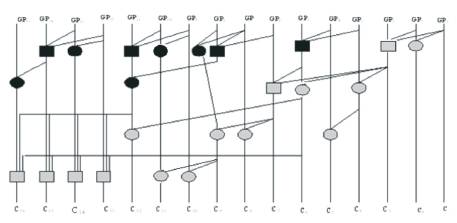
Figure 5. Hybrid 16-bit parallel prefix adder [28]
Steps for implementation of Transposed form of FIR filter shown in Figure 2 are:
The transposed form of 4-tap FIR filter is simulated using Xilinx 14.5 version by writing VHDL Code and implemented with the targeted device XC3S500E. The addition operation is done by using parallel prefix adder (16-bit). The multiplier (8-bit) unit is also developed, using Shift-andadd technique, which internally use parallel prefix adder for an addition operation. These developed components of parallel prefix adder and multiplier block are used in the FIR filter implementation. The input samples of FIR filter are considered for 8-bit width, the multiplier is designed for (8X8) size, the parallel-prefix adder for 16-bit are considered for filter implementation.
The results of FIR filter, based on various parallel prefix adder variants are tabulated in Table 1. The comparison is done for three factors: speed, area and power consumption. The speed performance is evaluated with respect to Maximum operating frequency and delay parameters. The area requirement can be estimated from the utilization of a number of slices and Look-up tables. The power consumption is analyzed by taking switching power (dynamic power) into account, which mainly depends on the input test vectors that can be applied through the test bench. Static power is not considered because ASIC tools are available.
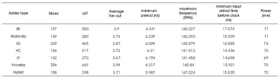
Table 1. Results of 4-tap FIR filter with various parallel prefix adder variants
The design summary of synthesis, power analysis and the results of hybrid parallel prefix added based, 4-tap FIR filter are given in Figure 6 and 7 respectively.
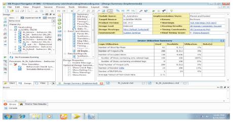
Figure 6. Design Summary of hybrid parallel prefix added based 4-tap FIR filer
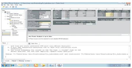
Figure 7. Power analysis results of hybrid parallel prefix added based 4-tap FIR filter
For better comparison of the results of FIR filter based on various parallel prefix adder implementations, these are presented in Figures 8 to 14 and in Table 2.
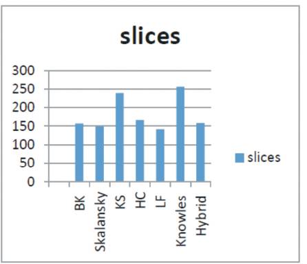
Figure 8. Utilization of Slices of 4-tap FIR filter with various adder variants
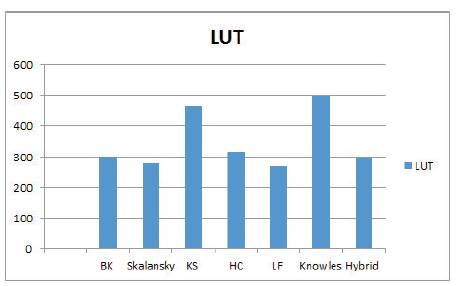
Figure 9. Utilization of LUTs of 4-tap FIR filter with various adder variants
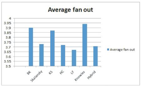
Figure 10. Average fan-out of 4-tap FIR filter with various adder variants
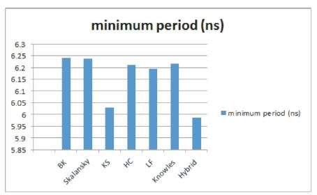
Figure 11. Average fan-out of 4-tap FIR filter with various adder variants
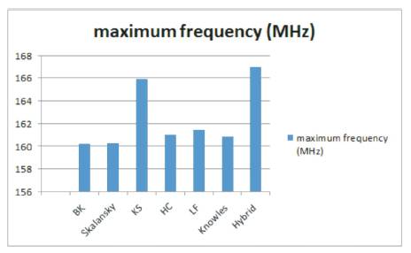
Figure 12. Maximum Clock frequency of 4-tap FIR filter with various adder variants
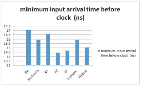
Figure 13. Minimum input arrival time requirement for clock of 4-tap FIR filter with various adder variants
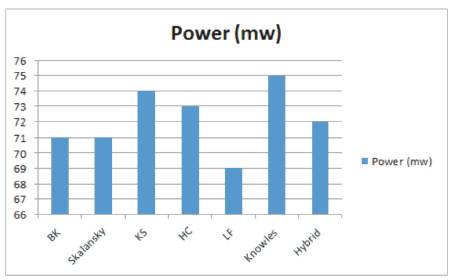
Figure 14. Dynamic power consumption of 4-tap FIR filter with various adder variants
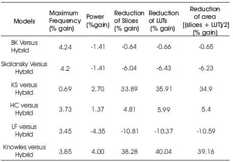
Table 2. Performance of 4-tap FIR filter using hybrid PPA when compared with other PPA variants
This paper presents the implementation of 4-tap FIR filter using MAC technique. The required addition and accumulation operations are performed by various parallel prefix adder variants. To evaluate the performance of this FIR filter, Xilinx 14.5 version of VHDL is used with the targeted device of Spartan 3E. The experimental results of 4-tap FIR filter based on hybrid PPA is compared with various PPA variants.
The speed of the FIR filter is estimated by the Maximum Frequency. The Maximum Frequency of FIR filter with hybrid PPA is 167.024MHz, which is high when compared to all other models. The frequency is almost 4% more than existing models except in KS which is 0.69%. The power consumption is less when compared with KS, HC, Knowles models, and a maximum of 4% power is saved when compared with Knowles model. The utilization of the area is less when compared to KS, HC and Knowles models. When compared with the LF model, hybrid model consumes more power (4.3%) and occupies more area (10.59%), but the speed of hybrid model is 3.45% greater.
The 4-tap FIR filter based on hybrid PPA shows superiority in all aspects when compared with KS, HC and Knowles models, among which maximum improvement in speed, power and area resulted when compared to Knowles model. Hence the implementation of FIR filter using hybrid PPA improves the performance of FIR filter in speed, power and area parameters.
The FIR filters are one of the important elements in digital signal processing applications. In particular, the use of FIR filter in digital communications in the IF stage of the receiver, allows the receivers a good noise rejection and the easy adjustment of incoming frequency without changing the hardware. The FIR filters designed in this paper will enhance the overall system performance. The performance of the FIR filter can be further estimated with higher order (or tapping) filters.