Memory Implementation Using Multi Bit Flip-Flop
Palagani Yellappa * Mareddi Bharathkumar** Shaik Shabana Azmi***
* ,** M.Tech Student, VLSI, Department of Electronics and Communication Engineering, Sree Vidyanikethan Engineering College, Tirupathi
*** Assistant Professor, VLSI, Department of Electronics and Communication Engineering, Annamacharya Institute of Technology & Sciences, Tirupathi..
Abstract
In the digital world memory elements play a vital role. In memory devices the most important factors are Area, Power and Speed. Increased Area and Power consumption of the memory device means reduced device reliability and lifetime. Flip-flops are the basic sequential components used for memory applications. D Flip-flop is one of the most commonly used Flip-flops and delay consumed by clocking is a major part of the whole design. In this paper, the authors analyze the design of Single-Bit Flip-Flop (SBFF i.e. 1-bit) and make a performance comparison over the Multi-Bit Flip-Flop (MBFF i.e. 2-bit, 4-bit, 8-bit, 16-bit and 32-bit). In this paper, the authors design SRAM and DRAM using both SBFF and MBFF in Xilinx Virtex-5 family (XC5VLX50). Designing the memory by using SBFF implies more power consumption. To get the maximum reduction in power and delay an algorithm has been proposed in which SBFFs are replaced with maximum possible MBFF without affecting the performance of the original circuit. These result in favor of Multi-Bit Flip-Flop as reduction of delay such as gate delay and net delay.
Keywords :
- Flip-Flop, SBFF (Single-Bit Flip-Flop)
- Merging
- Area
- Delay
- SRAM (Static Random Access Memory)
- and DRAM (Dynamic Random Access Memory)
Introduction
Optimizations in VLSI have been done on three factors Power, Area and Time (Speed). To optimize the power consumption, many Low-power design techniques have been introduced such as power gating, clock-gating, dynamic voltage/frequency scaling and minimizing clock network. Minimizing clock network technique is a very important one for reducing power consumption. Area optimization means reduction of the space of a Digital design[1] . Timing Optimization is also another important one in the modern VLSI world.
Flip-flops mainly include positive and negative pulseedge triggering methods. When a Flip-flop is required to respond at a LOW to HIGH transition state, a positive- edge pulse triggering method is used. When a Flip-flop is required to respond during the HIGH to LOW transition state, a negative-edge pulse triggering method is used.
MBFFs is an effective method to reduce clock power consumption. MBFFs can significantly reduce the number of individual loads on the clock tree, reducing overall dynamic power used in the clock tree [2] [3] . Area and leakage power savings can also be achieved simply by sharing the clock inverters in the Flip-flops within a single structure is shown in Figure 1.
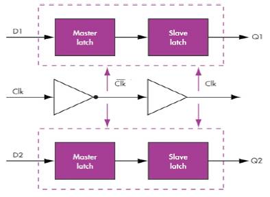
Figure 1. Combining two single-bit flops into a dual flop with shared clocking
The rest of this paper is organized as follows. The authors briefly discuss SBFF and MBFF methods in Section 1. The memory implementation (SRAM and DRAM) along with possible 4k-bit hardware implementations and their analysis are described in Section 2. In Section 3 SBFF and MBFF are simulated and verified using Verilog HDL in Xilinx ISE 10.1i for the target device xc3s500e-5fg320. Finally, this paper contains the conclusion section.
1. SBFF and MBFF
Flip-flops and Latches are the fundamental building block of Digital electronics systems used in computers, communications and many other types of systems. Flipflops and latches are used as data storage elements. The main differences between Flip-flops and latches are shown in Table 1. Latch is asynchronous and their outputs change immediately when their inputs change[4] . Flipflops on the other hand, have their content changed only either at the rising or falling edge of the enabling signal. This enabling signal usually controls the clock signal. After the rising or falling edge of the clock, the Flip-flop content remains constant even if the input changes.
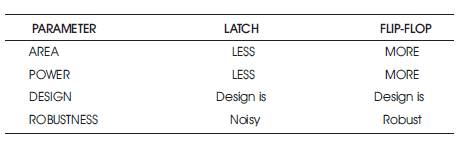
Table 1. Difference between Latch and Flip-Flop
In this section, the authors have introduced SBFF and MBFF concepts. Before that, they review SBFF (1-bit). It has a single input called the 'DATA' input. D Flip-flop is one of the most commonly used Flip-flops. For a positive-edge triggered D Flip-flop, its output Q follows input D only at every L to H transition of CLOCK, otherwise Q keeps unchanged. The RTL schematic of SBFF (1-bit) is shown in Figure 2.
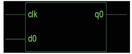
Figure 2. RTL schematic of Single bit Flip-flop (1- bit)
The working of D Flip-flop is similar to the D latch except that the output of D Flip-flop takes the state of the D input at the moment of a positive-edge at the clock pin (or negative-edge if the clock input is active low) and delays it by one clock cycle. That's why, it is commonly known as a “Delay Flip-flop”. The D Flip-Flop can be interpreted as a delay line or zero order hold. The advantage of the D Flipflop over the D-type "transparent latch" is that the signal on the D input pin is captured the moment the Flip-flop is clocked and subsequent changes on the D input will be ignored until the next clock event. From the timing diagram (Figure 3), it is clear that the output Q changes only at the positive edge.
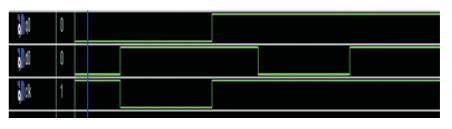
Figure 3. Timing diagram for SBFF
At each positive edge, the output Q becomes equal to the input D at that instant and this value of Q is held until the next positive edge
A SBFF has two latches (Master latch and slave latch). The latches need “Clk” and “Clk'” signal to perform operations. For improving Flip-flop performance, one of the promising way is, to merge the clock pulse. The MBFF is designed by single clock pulse and achieves the same functionality as two SBFFs. Figure 4 shows, merging two single-bit Flip-flops into one 2-bit Flip-flop[5][6]and the total power consumption can be reduced because the two single-bit flip-flops can share the same clock buffer.
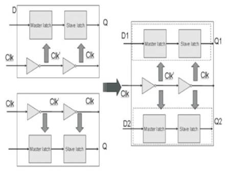
Figure 4. Merging two single-bit Flip-flops into one 2-bit Flip-flop
MBFF (2-bit, 4-bit, 16-bit and 32-bit) has two or more inputs. MBFF takes multiple data input and results in multiple data output. The working of MBFF is same as SBFF, whenever the clock gets active state Flip-flop latches all input to output. For inactive state the Flip-flop holds the data. For example consider 2-bit Flip-flop, it has 2 inputs and 2 outputs shown in Figure 5.
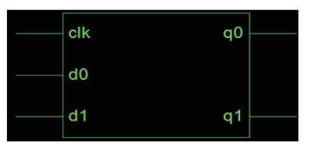
Figure 5. RTL schematic of multi bit Flip-flop (2- bit)
MBFFs may offer many advantages as follows:
- Area and delay is reduced
- Number of inverters is reduced in clock sinks
- Routing resource utilization is improved
2. Memory Implementation
Random Access Memories (RAM) may store information in Flip-flop style circuits or simply as charge on capacitors. Approximately equal delays are encountered in reading or writing data. Because read-write memories store data in active circuits, they are volatile, that is, stored information is lost if the power supply is interrupted. The two most common types of RAMs are the static RAM (SRAM) and the dynamic RAM (DRAM).
2.1 SRAM
It is known as Static Random Access Memory and its operation is very much important in the memory design. The operation can be in Bit-oriented manner or in Wordoriented manner [7] . In Bit-oriented manner we access the data in a single bit manner but in word-oriented, as multiple bits in terms of powers of 2. So Word-oriented is little bit complex rather than Bit-oriented. SRAM is a more important electronics component in the day to day market. Now a days people want minimum cost, easy availability and proper functioning, so that a custumer can easily handle the data and properly utilize it for future uses also. The important thing in the design of SRAM cell is that it needs low power and low man power for designing.
The data storage in SRAM depends on the DC source. If the DC source is removed, the data can be erased. SRAM 4k-bit has its own input and output lines, and control signals WRITE and PHI_B. It is designed with 8 rows and 4 columns [8] as shown in Figure 6.
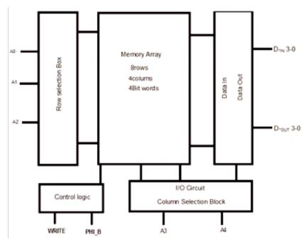
Figure 6. 4k-bit SRAM Functional block diagram
Data is read out or written into memory in the form of 4-bit words. 3 address bits are required to decode a row and 2 bits are required to access a word in a column. Each SRAM cell has a word line and two bit-charge lines and fully operates in static mode. Therefore, no clock or refreshment is required. Testing for 4k-bit SRAM flows along the functional blocks address decoders, SRAM cell and multiplexers [9]. The pin description for SRAM is shown in Table 2.
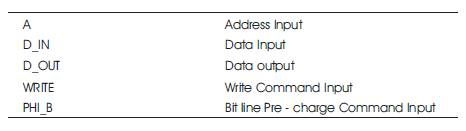
Table 2. Pin description
SRAM cell has four cases for its operation; read “1” or “0”, write “1” or “0”, all of these cases were tested using Xilinx Virtex-5 family. Because SRAM cell requires a sort of tuned timing for input signals, each of PHI_B, WL, WRITE and DATAIN were set up to meet this requirement. By using address lines the Flip-flop is selected to write or read the data. The operation of the SRAM is: when r=0, the write operation is done. When r=1, the read operation is performed.
2.2 DRAM
The first-generation DRAMs include multiplexed address inputs, multiple memory arrays and the 1-transistor/1- capacitor memory cell. Furthermore, second-generation DRAMs offer more modes of operation for greater flexibility or higher speed operation. The 4k-bit DRAM Functional block diagram is shown in Figure 7.
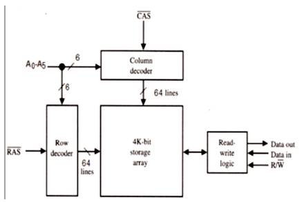
Figure 7. 4k-bit DRAM Functional block diagram
DRAM is known as Dynamic Random Access Memory and second-generation DRAMs range in size from 4k (4,096 x 1 bit, i.e.4096 address locations with 1-bit input/output word size) up to 64 Meg (67,108,864 bits) in memory sizes of 16 Meg x 4 organized as 16,777,216 address locations with 4-bit input/output word size 8 Meg x 8 or 4 Meg x 16. DRAM 4k-bit has own input and output lines and has read logic and write logic [10] . The Row Address Strobe (RAS) input clocks the address present on the DRAM address pins Ao to A5 into the row address latches on the falling edge. The Column Address Strobe (CAS) input clocks the input address into the column address latches on its falling edge. Table 3 shows the pin description for DRAM.
Table 3. Pin description
3. Results and Discussion
The proposed system is simulated and verified using Verilog HDL in Xlinix ISE 10.1i for the target device xc3s500e-5fg320.
3.1 SBFF and MBFF Results
Figures 8 to 12 show the simulation results and outputs of the SBFF and MBFF. The constraints taken to consideration are number of IOs, number of bonded IOBs, IO buffer (IBUF and OBUF) and delay path (gate delay and net delay).
Figure 8. Simulation result for single-bit Flip-flop (1-bit)
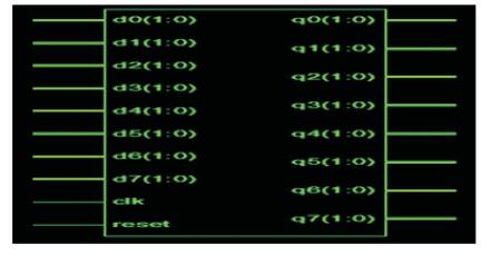
Figure 9. RTL Schematic of MBFF (8-bit)
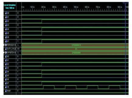
Figure 10. Simulation result for multi-bit Flip-flop (8-bit)
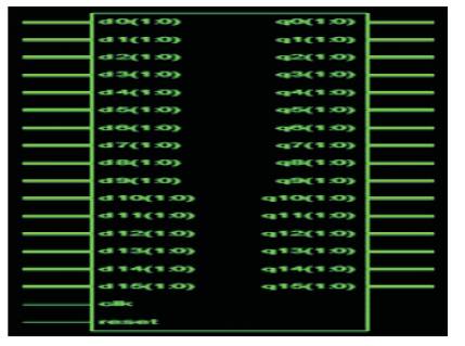
Figure 11. RTL Schematic of MBFF (16-bit)
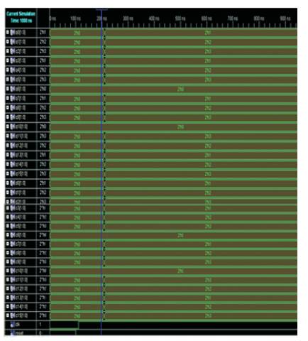
Figure 12. Simulation result for multi-bit Flip-flop (16-bit)
Experimental results indicate that multi-bit Flip-flop is very effective and efficient method in lower-power designs. Table 4 shows the comparison of SBFF (1 bit) and MBFF (2- bit, 4-bit).
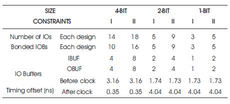
Table 4. Comparison of SBFF (1-bit) and MBFF (2-bit, 4 bit)
3.2 RAM Results
The analysis of RAM (SRAM and DRAM) is done using MBFF and is targeted and verified on Xilinx FPGA of family Spartan-3E. Table 5 shows the comparison of 8-bit, 16-bit and 32-bit MBFF. The number of Flip-flops in SRAM using SBFF is about half the number in SRAM using MBFF. The RTL schematic consist of two input lines (Bit-line and Word-line) as shown in Figure13 and simulation result is shown in Figure14. The strategies are minimizing the delay and power dissipation as shown in Table 6.
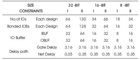
Table 5. Comparison of MBFF (8-bit, 16-bit and 32-bit)
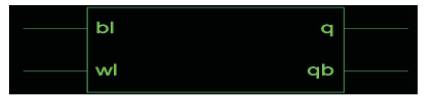
Figure 13. RTL schematic of SRAM
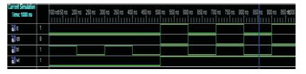
Figure 14. Simulation result for SRAM
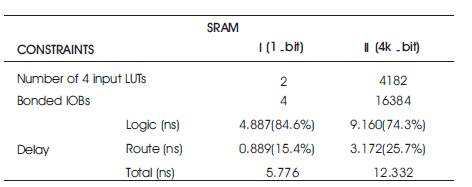
Table 6. Comparison of 1-bit SRAM and 4k-bit SRAM
Conclusion
In present VLSI design, area is one of the major issues to be addressed. To achieve reduced area various types of Flipflops and RAMs are discussed. The SBFF consumes more power because of inverters in clock sinks, so to reduce this power consumption, MBFF is designed. Here Xilinx FPGA of family Spartan-3E tool is used to design the SRAM and DRAM using MBFF. The Area and Delay Analysis Reports indicate that MBFF in combination with SRAM and DRAM is very effective and efficient method in lower-power designs.
References
[1]. G.Prakash, K.Sathishkumar, S.Saravanan, (2013). “Achieveing reduced area by multi-bit Flip Flop design” International Conference on Computer Communication and informatics.
[2]. LI Xia Yu, JIA Song, LIU LiMin, (2012). “Design of Novel, Semi- transparent Flip-flops for high speed and low power application”, Science China Information Sciences, Vol. 55.
[3]. K. Siva Prasad, G. Rajesh, V. Thrimurthulu, (2014). "Implemenation of MBFF power reduction in CMOS technologies" IJIRCCE, Vol. 2, Special Issue 4.
[4]. B. Saibabu, K. Sudha Rani (2014). "Design and Analysis on Single-Bit to Multi-Bit Flip Flop" IJSETR, Vol. 03,Issue. 24.
[5]. Challa Sankaramma, K. D. Mohana Sundharam, (2014). “Optimization of area through multi bit Flip-flop th design using FPGA” IRF International Conference, 14 December, Chennai, India.
[6]. K. Sarada mani, R. P. Rubajini (2014). "Application of Multibit Flip-Flops by Using Carry Look Ahead Adder" IJETAE Vol 4, No 1.
[7]. M.Ananthi, C.Sathish Kumar (2015). "QDR SRAM Design Using Multi - bit Flip-Flop" IJARECE, Vol 4, No 3
[8]. Joonsung yang/ Gahngsoo Moon, (2005). “32k-bit sleepy SRAM”, in Benton H. Calhoun, Frank A. Honore, Anantha P. Chandrakasan- (2004). “A Leakage reduction methodology for distributed MTCMOS”. IEEE Journal of Solid state circuits, Vol. 39, No.5.
[9]. K. Ravi Teja Kumar, K. Ramesh (2015). "Implementation of SRAM array by using MBFF" IJRCAR Vol.3 No. 4.
[10]. Charles Kime & Thomas Kaminski, (2008). “Logic and Computer Design Fundamentals” Pearson Education, Inc.