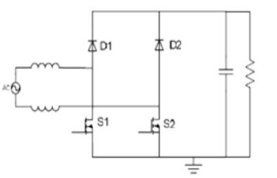
Figure 1. Bridgeless PFC Circuit
To reduce the rectifier bridge conduction loss, different topologies have been developed. Among these topologies, the bridgeless boost does not require range switch and shows both simplicity and high performance. Without the input rectifier bridge, bridgeless PFC generates less conduction loss as compared to the conventional PFC. Although the circuit structure is simple, the location of the boost inductor on the AC side makes it difficult to sense the AC line voltage and inductor current. At the same time, since the AC side inductor structure makes the output floating regarding the input line, the circuit suffers from high common mode noise. Compared to the average current mode control, one cycle control shows many benefits such as no multiplier requirement, no input voltage sensing requirement, and no inductor current sensing requirement. Therefore, one cycle control gives an attractive solution for the bridgeless PFC circuit. In this paper, One Cycle Control technique is implemented in the bridgeless PFC. By using one cycle control both the voltage sensing and current sensing issues of the bridgeless PFC circuit can be solved. The experimental results show both efficiency improvement and good power factor correction function. At the same time EMI results show that the circuit noise is controllable.
Single switch CCM PFC [6] is the most widely used topology for PFC applications because of its simplicity and smaller EMI [5] filter size. Due to the high conduction loss and switching loss, this circuit has low efficiency at low input line. With the development of super junction MOSFET and SiC Schottky diode, switching loss of the PFC circuit is dramatically improved. Meanwhile, the circuit still suffers from forward voltage drop [3] of the rectifier bridge which causes high conduction loss, especially at low input line.
By using one cycle control both the voltage sensing and current sensing issues of the bridgeless PFC[1] circuit can be solved. The experimental results show both efficiency improvement and good power factor correction[8,9] function. At the same time EMI [7] results show that the circuit noise is controllable.
The bridgeless PFC circuit is shown in Figure 1. The boost inductor is split and located at the AC side to construct the boost structure. The equivalent circuit of positive half line cycle is shown in Figure 2. In this half line cycle, MOSFET S1 and boost diode D1, together with the boost inductor form a boost DC/DC converter. Meanwhile, MOSFET S2 is operating as a simple diode. The input current is controlled by the boost converter and depends on the input voltage.
Figure 1. Bridgeless PFC Circuit
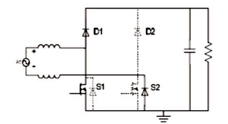
Figure 2. Equivalent Circuit of Bridgeless PFC
During the other half line cycle, circuit operates in the same way. Thus, in each half line cycle, one of the MOSFET operates as active switch and the other one operates as a diode: both the MOSFETs can be driven by the same signal.
The difference between the bridgeless PFC and conventional PFC is summarized in Table 1. Comparing the conduction path of these two circuits, at every moment, bridgeless PFC inductor current only goes through two semiconductor devices, but inductor current goes through three semiconductor devices for the conventional PFC circuit.
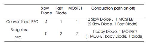
Table 1. Differences b/w conventional & bridgeles PFC
As shown in Table 1, the bridgeless PFC uses one MOSFET body diode to replace the two slow diodes of the conventional PFC. Since both the circuits operate as a boost DC/DC converter, the switching loss should be the same. Thus the efficiency improvement relies on the conduction loss difference between the two slow diodes and the body diode[11] of the MOSFET. Besides, compared with the conventional PFC, the bridgeless PFC not only reduces conduction loss [2], but also reduces total components count.
To estimate the efficiency improvement by using bridgeless PFC circuit [4], the loss comparison is performed based on a theoretical analysis. The switch of choice is a super junction MOSFET rated at 22A, 600V and the diode bridge is chosen as GBPC2506W, rated at 25A, 600V. Curve fitting method is used to generate the conduction loss model of these devices. Based on the inductor instantaneous current, the conduction losses generated by these two devices at 90V input and different output power are calculated as shown in Figure 3.
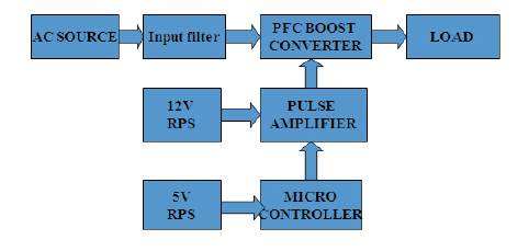
Figure 3. Block Diagram of Bridgeless PFC
For all the power level ranges, bridgeless PFC can improve the total efficiency[10] at the full power level by around 1%. Considering small MOSFET on state resistance, turning on the MOSFET may further reduce the conduction loss by using synchronous rectifier. The conduction loss of the MOSFET is evaluated based on the lower voltage drop caused by the MOSFET body diode and on the state resistance. The power losses of these two cases are very similar.
AC source provides supply to rectifier. The input side has one inductive filter. It is used to improve the input power factor.
It converts AC supply to DC supply. DC supply has some ripples. It is filtered with the help of capacitor filter. input voltage is boosted by controlling the pulse width of the rectifier.
The output has DC output votlage. It is used to run motors, battery charging and telecommunication applications.
Micro controller is used to generate triggering pulse for MOSFETs. It is used to control the outputs. Micro controller has more advantages compared to analog circuits and micro processors, such as fast response, low cost, small size etc.
It is also called power amplifier because it is used to amplify the pulse output from micro controller. It is also called as opto coupler IC. It provides isolation between microcontroller and power circuits.
RPS gives 5V supply for micro controller and 12V supply for driver. It is converted from AC supply. AC supply is stepped down using step down transformer.
For the conventional PFC, input voltage sensing is simple. The rectified input voltage can be directly sensed by using the voltage divider, because of the existence of the rectifier bridge. EMI noise issues rely on the power stage structure.
For the conventional PFC, the output voltage ground is always connected with the input line, through the rectifier bridge. Therefore, the parasitic capacitor contributes to the common mode noise by way of parasitic capacitance between the MOSFET drain to the earth ground.
For the bridgeless PFC the output voltage is always floating in regard to the input AC line. Thus, not only the parasitic capacitance between the MOSFET drains to the earth ground Cd1 and Cd2, but also all the parasitic capacitances between the output terminals to the earth ground Cn and Cp contribute to the common mode noise, as shown in Figure 4.
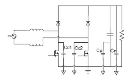
Figure 4. Parasitic Capacitances that contribute to common mode noise for bridgeless PFC
As the dv/dt of the parasitic capacitances between the output terminals to the earth ground, Vp and Vn, are the same, there is no way to achieve noise cancellation. Considering that these capacitors not only include the output of the PFC stage parasitic but also the input for the load, the common mode noise can be much worse as compared to the conventional PFC circuit.
To solve the EMI noise issue, a new EMI noise reduction circuit for the bridgeless PFC circuit is introduced. The circuit schematic is shown in Figure 5. As compared to the original bridgeless PFC circuit, the circuit adds two capacitors in the circuit to create a high frequency path between the output voltages to the input AC line.
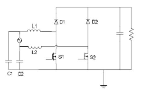
Figure 5. An Improved EMI Performance Bridgeless PFC Circuit
Figure 6 shows the circuit diagram of conventional boost converter. Figure 7 shows the applied AC input voltage and current. The conventional boost converter gives the simulation results as output current and output voltage which are shown in Figure 8 and Figure 9.
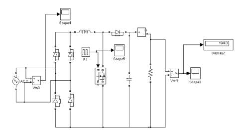
Figure 6. Conventional boost converter
Figure 7. Ac input voltage and current
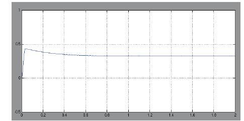
Figure 8. Output current
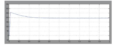
Figure 9. Output voltage
Figure 10 shows the circuit diagram of the proposed boost converter. Figure 11 shows the applied AC input voltage and current. The proposed boost converter gives the simulation results as output current and output voltage which are shown in Figure 12 and Figure 13.
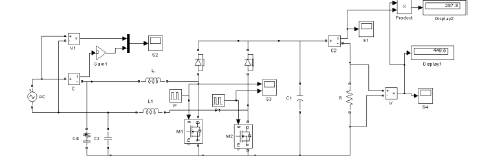
Figure 10. Proposed boost converter
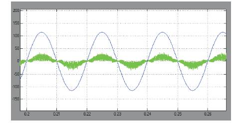
Figure 11. Ac input voltage and current
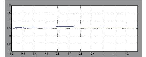
Figure 12. Output current
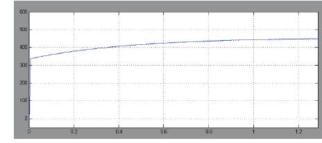
Figure 13. Output voltage
Figure 14 shows the circuit diagram of proposed boost converter with RL load. Figure 15 shows the applied AC input voltage and current. The proposed boost converter with RL load gives the simulation results as output current and output voltage which are shown in Figure 16 and Figure 17.
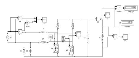
Figure 14. Proposed boost converter with RL load
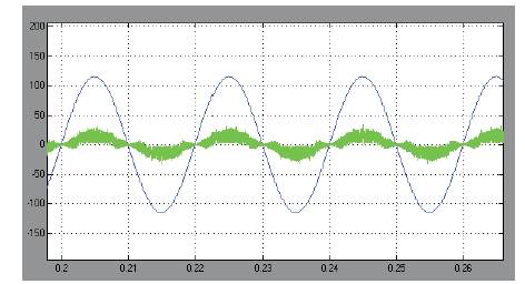
Figure 15. Ac input voltage and current
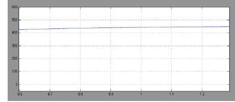
Figure 16. Output voltage
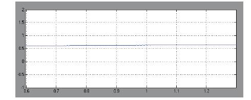
Figure 17. Output current
Figure 18 shows the circuit diagram of the proposed boost converter with RL load for the open loop mode. Figure 19 shows the input and output voltage for open loop mode. Figure 20 shows the circuit diagram of the proposed boost converter with RL load for the closed loop mode. Figure 21 shows the input and output voltage for closed loop mode.
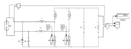
Figure 18. Circuit diagram for open loop
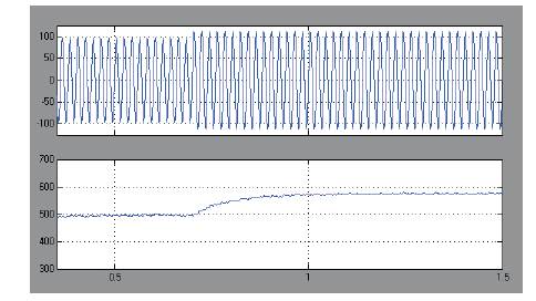
Figure 19. Input and output voltage for open loop
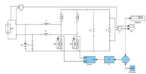
Figure 20. Circuit diagram for closed loop
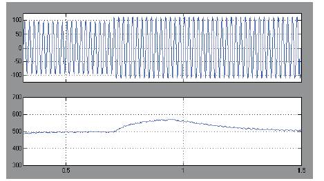
Figure 21. Input and output voltage for closed loop
The proposed circuit is simulated using MATLAB. Both bridge boost converter and bridgeless boost converters were simulated. Bridgeless boost converter has high performance compared to the dual-boost PFC rectifier that employs a multiple-winding magnetic device to increase the utilization of the magnetic core that has been introduced. The performance of the proposed rectifier was verified by experimental prototype. The proposed technique improves the efficiency by approximately 1% compared to the conventional PFC boost rectifier, and improves the utilization of the magnetic cores from the conventional bridgeless dualboost rectifier, resulting in a low-cost high-power-density design.