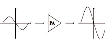
Figure 1. Basic Amplifier Function
In wireless transmission systems, non-ideal response of different functional components along with non linearity of power amplifier plays a major role in degrading the transmitter performance. Several parameters define the performance of a wireless, such as Adjacent Channel Power Ratio (ACPR), Error Vector Magnitude (EVM), spectral mask, etc., and the effect of non-ideal behavior of the transmitter affects these parameters. In many standards, these parameter specifications are defined such that the concern for transmitter linearization is very much relaxed. Standards like Terrestrial Trunked Radio (TETRA) specify strict regulation on these parameters. Therefore, the requirement of linearity is a great challenge for the design of a transmitter, and among these the Digital Pre-distortion (DPD) technique is a wellknown concept. In this paper, an appropriate architecture of SDR is presented for successful operation of the DPD technique. Both signal processing and physical layer architecture may be utilized for complete implementation of the SDR system.
Radio Frequency (RF) communication has surged in the recent years. Research activities in the area of RF communication have become very popular. In response to the demand of efficient, high data rate transmitters, research on commercially applicable transmission system has got massive attention. Given the market demand for a flexible and user-friendly transmitting device, meeting the technical challenges within the radio standard requirements is an important aspect of communication performance. Every communication standard has its own specification of performance metrics and definitions of transmission parameters. Any implementation and organization of transmission system needs to follow the standard specific parameter definitions. Therefore, to construct a transmission concept or implement any transmission system, full standardization of the overall transmission system is needed, according to the requirement.
Designing a transmission system concept with ideal transmit components involves less concern as compared to the conformance to the standard. Non-ideal transmit-path components introduce distortions to the ideal transmit signal, and these distortions produce spectral components that are beyond the allocated bandwidth. Any counter measure used for eliminating the senonideality from the transmit-path is called linearization
Signal distortion is, by definition, an unexpected change in the form of a signal which causes degradation of the signal quality during transmission. Distortion can occur at different stages of transmission, such as in the base band signal generator, filtering, RF modulator, power amplifier, etc.. The major portion of the distortion is caused by the RF Power Amplifier (PA) which is a final-stage active component of the system. The quality of the signal needs to be as ideal as possible at the output of the PA as it is considered as the final output of the transmitter. In most of the literature about linearization, RF power amplifier has been assumed to be the only nonlinear component of the transmitter. As the power amplifier shows very significant nonlinearity for high power applications, much of the linearization work has been done to eliminate the effect of non linearity.
The primary objective of this paper is to explain the nonlinear distortion associated with power amplifier, and to present an appropriate Software Defined Radio (SDR) system to rectify the problem of non-linearity using Digital Pre-distortion Technique (DPD) [1]-[5].
Due to the nonlinearity of the power amplifier, and other distortion caused by the transmitter, the output of the transmitter experiences different types of signal alteration. There might be out-of-band signal component in the transmitting wave form as a swell in the distortion component within the expected transmission band. Spectral regrowth or spurious emission can be harmful for the devices operating on adjacent frequency band. When there is distortion within the band width, there will be constellation error. Neither of the distortions is desired, and therefore these need to be minimized. Description of several types of distortion is given below.
Figure 1. Basic Amplifier Function
Nonlinear distortion of the transmit signal mainly arises from the RF power amplifier nonlinearity. Normally, the nonlinearity arises from a non-constant gain response from the power amplifier. Non-constant envelope signals have a large signal variation which results in variable amounts of signal throughout the amplification. A perfect amplifier would have a perfect linear transfer characteristic, and the output gives a scaled or amplified version of the given input signal. Figure 1 shows basic PA characteristics. Linear response is defined by

Where, A is the signal gain of the amplifier. There will be no distortion of the waveform at the output of the amplifier. We can describe the nonlinear distortion of a power amplifier with no memory effect by power series function,
If the input signal of the power amplifier is used in the power-series function, we obtain,

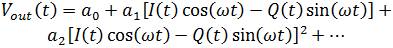
Therefore, we can define the nonlinear function as a function of the input signal. After RF modulation, the I and Q path are combined which would then be applied to the input of RF power amplifier. Figure 2 shows quadrature modulation overview of system architecture. The combined signal expression is given by,

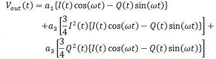
Now, if we use S(t) as input signal in power series expansion of equation (3) to describe the transmitter distortion, we obtain the following,
After harmonic filtering, and considering up to third order components, we have
We obtain the Gain function by following,

Therefore, it can be said that the baseband I and Q signals experience a non-constant gain. It may also be observed from the polynomial that the RF carrier is modulated by every odd order baseband signal component, where it is expected that every higher order of carrier harmonics are filtered out. As such, the modulated RF signal has strong odd order baseband signal component. Thus, the band of baseband spectrum spreads to the adjacent channels. If this spectral regrowth is not compensated, we can have a serious ACPR issue.
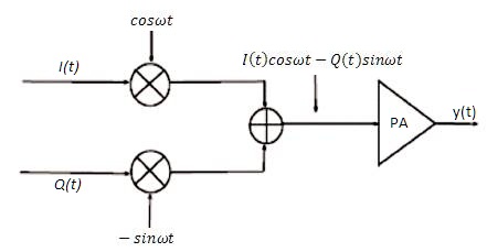
Figure 2. Modulating Signal Path.
The nonlinearity of an RF power amplifier can be described by Amplitude Modulation (AM) and Phase Modulation (PM) characteristics of the output waveform of the RF power amplifier. Occurrence of AM distortion at the output is usually called AM/AM distortion, and similarly PM distortion at the output is called AM/PM distortion. The nonlinear relationship between input power and the output power causes the “AM/AM” effect. The other type of distortion, AM/PM, is caused by phase modulation of the input signal, which refers to the conversion of the AM modulated signal at the input waveform to the phase modulated signal at the output. Consider a modulating signal to be defined by,

Where, A is the signal amplitude, and w, the frequency of b the cosine signal. In the case of ideal amplification, the output phase should be given by,

where KΦ is a constant, and V(n)t is the modulated carrier. That means, the output phase of the amplifier keeps constant. Therefore, we obtain a linear input-output relationship given by

Where, G is the ideal gain of the amplifier and ωc is the angular frequency of the RF signal.
Due to distortion in the PA, the Amplitude Modulation (AM) present in the input signal will result in phase modulation of the output signal.
This modulation transform [6] . is described by
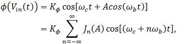
Where Jn is the Bessel function of order n and ωc is the angular frequency of the RF carrier
The cause of AM/PM distortion may be due to nonlinear phase characteristics of the amplifier. When the amplifier delays different frequency components by different values, then it is termed as nonlinear phase response
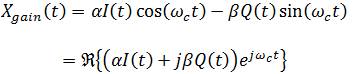
Digitally modulated baseband signal travels in two paths, which are mixed with RF carrier in quadrature, and is then combined to provide a single output signal. If the gain in the independent I and Q path are not matched, i.e., is unequal, then there will be distortion in the symbolconstellation. This type of distortion is called gain mismatch or IQ imbalance. We consider α and β to be gains of I and Q channels respectively. Then, the combined signal after modulation in given by
It can be observed from Figure 3 that the Iand Q components of the signal constellation have different gains due to IQ imbalance.
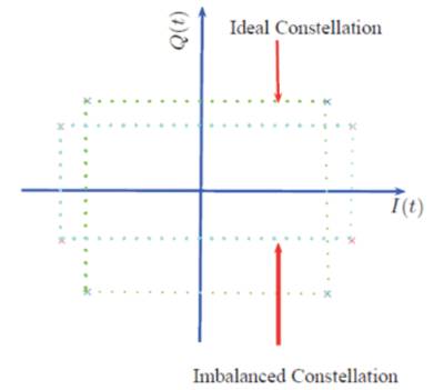
Figure 3. Modulating Signal Path.
Due to non-ideal RF components:
RF modulator, combiner and power amplifier, we may have non-orthogonal distortion. This distortion results in coupling of two baseband signals: I(t) and Q(t) as shown in Figure 4.
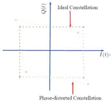
Figure 4. Quadrature Phase-distortion of 4-QAM
This can be described mathematically as
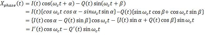
Therefore, due to quadrature phase distortion in the transmit path, we get coupled I’ and Q’

Phase error is produced while splitting Local Oscillator (LO) signal into sine and cosine. As these errors add linearly to the original signal, its inversion coefficients can easily be known. The coefficients can be adaptively determined by observing the IQ plane. The compensation of non-ideal behavior will be discussed in detail later. Note that these effects do not show up in the frequency spectrum.
I (t) and Q (t) input signals to the modulator may contain DC components, and its effect can be seen in the constellation and transmit signal as shown in Figure 5. The output is expressed as,

Ioffset + j Qoffset gives modulated signal offset offset with extra carrier [7]. This is called carrier leakage. The reason for DC offset can be that of DACs or other baseband circuitry before modulator.
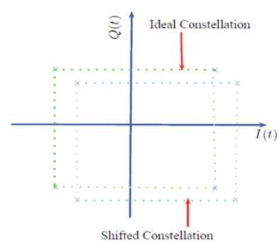
Figure 5. Carrier Leakage
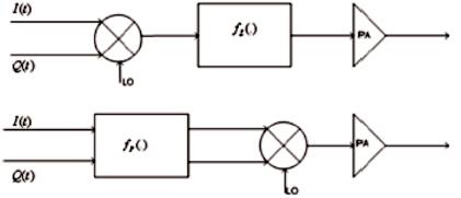
Figure 6. Predistortion technique for Linearization
There are several elements that may be used to successfully implement the proposed SDR model. Proper utilization of DPD technique can be achieved by the cost of signal processing power.
The novelty of the architecture is its capability of adjusting the look-up tables over time through on-demand calibration routine. In order to perform a successful transmitter calibration, an additional hardware deployment is proposed.
The fundamental principle of the predistortion is to introduce a pre-distorter or post-distorter such that the combination provides a linear function. Predistortion can be applied at the both RF and digital level. RF predistortion is quite similar to feed-forward linearization scheme, whereas digital predistortionis are employed at the digital level for predistortion of the baseband signals. Digital predistortion makes use of the improvement in the processing power of DSP devices. Digital processing allows the baseband signal to be modeled in such a way that it can counter the nonlinear model of the power amplifier and other nonlinear devices.
The two most common types of pre-distorter are: mapping pre-distorters and constant-gain pre-distorters. Mapping predistorter requires two look-up tables which are functions of two variables (i.e., I and Q). On the other hand, constant-gain pre-distorter uses a one-dimensional look-up table.
Figure 6 shows the predistortion concept with implementation in RF (top half) and baseband level (bottom half). The RF predistortion is done using a inverse characterization of the power amplifier after RF modulation. The detailed realization of the analog inverse is described in [8], [9] and[10] . The baseband predistortion is managed by digital look-up table. This method is described in detail in[3]
In this case, the predistortion with two look-up tables is considered. The look-up tables are assigned distortion values in two Cartesian coordinates, i.e., I and Q. In order to do so, the transmitter needs to go through a standard calibration process that ensures that the transmitter is maintaining its transmission quality requirement
The predistortion data is collected by sampling the transmitter's output at the power amplifier by a directional coupler and by demodulating the signal to its original symbol. Each symbol of the overall constellation is transmitted and compared to the original symbol. The error is calculated in two coordinates of the constellation, and thus two look-up compensation tables are created. For proper statistics of symbol errors, sufficient number of symbols of each constellation point needs to be transmitted. The averaged pre-distortion values would be applied to the signal for linearizing the nonlinear effect of the transmitter.
The symbols to be transmitted during the calibration stage can be assigned like a train of impulses as

where M is the number of symbols to be transmitted and T is the duration between two symbols.
In order to set the transmitter hardware to a proper state for secure transmission, a proper calibration routine should be run. The predistortion look-up tables are calculated during the process of calibration. Various other values are set for the transmitter during the calibration such as channel power calculation, forward path power attenuation setting, error vector magnitude calculation, removing modulator error, DC offset compensation etc..
With EVM calculation, the actual error in the demodulated symbol constellation is measured. The demodulated signal is mapped using the IQ constellation, and is compared with the actual symbol constellation point. For calculation of EVM, we first need to calculate the Signal Error Vector (SVE):
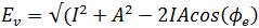
Where, I is the magnitude of ideal vector, A is the magnitude of measured vector, and Φ is the phase error between I and A. The measured vector magnitude, A, is composed of the reference vector magnitude, I, plus a component resulting from the gain error present in the system Ge

If the reference vector magnitude is normalized, then the resultant error vector magnitude, Evm can be defined as:

The GSM specification for EDGE modulation requires rms EVM to be below 9%, where 95% of symbols have EVM below 15%. The TETRA specification requires EVM to be less than 10%.
The RF signal is modulated with I and Q signals, and problems may arise with Direct Conversion Modulation (DCM), where modulation provides some discrete spurious, harmonic oscillations and phase noise. Discrete spurious are the spectral components that occur in discrete form at different frequency offsets from the carrier, and can be attributed to the parasitic and sub harmonic oscillations. Therefore, this type of unwanted frequency modulation would limit the ACPR performance of the transmitter. To avoid this type of distortion, there are several alternative solutions available. One solution suggests using an intermediate frequency before the actual RF modulation. If there is any non-orthogonality in the RF modulators, the signal would experience phase error.
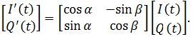
With phase error in the transmitter, the output signal constellation would have quadrature error within the symbol constellation. The signal with quadrature error is given by

Where, I’(t) and Q’(t) are the coupled baseband signals. The two distorted baseband signal can be expressed with the matrix form
Therefore, the non-orthogonality of the modulator can be attributed to the non-orthogonal operator,

By taking the inverse we can mitigate the effect of the nonorthogonal factor, Z. The inverse matrix is deduced as follows:
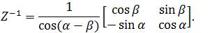
Applying Z-1 compensation to the I and Q signal before the modulator, the coupling problem due to nonorthogonality can be equalized. Therefore, with the compensation scheme we obtain the following:
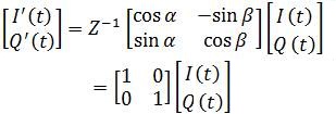
The compensation-inverse can be applied at physical layer before the RF modulation. In Figure 7, a compensation circuit is shown for making inverse of the non-orthogonal matrix. The coefficients are:
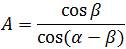
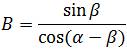
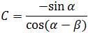
and
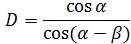
This compensating inverse may also be applied in digital level, and in that case the circuit shown in Figure 7 and it can be treated as digital algorithm of inversion process. Hence, using the proposed compensation circuit, it can be expected that the coupling of the non-orthogonal response would be equalized.
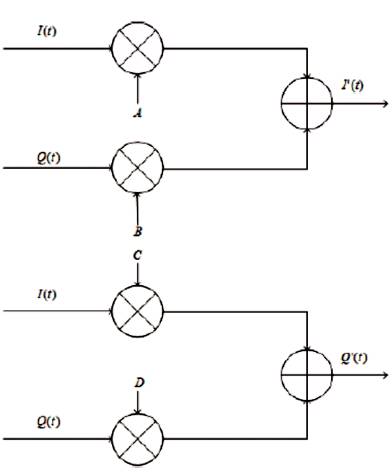
Figure 7. Compensation circuit for orthogonality- error
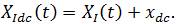
In the baseband circuitry with DC offset well above a certain level, the output of the amplifier would saturate, causing serious distortion. The other concern of the DC offset relates to the signal constellation. With the offset in the modulating signal, the modulator would give carrier leakage which in turn can be treated as part of the distortion. In order to nullify an arbitrary DC offset Xdc , we need to apply a DC offset to the generated baseband signal which in turn becomes an additional signal component of the original baseband signal. Thereby, the compensated
The matching of gain in the I and Q channels is another important factor for designing the transmitter. When the I and Q channels give two different gains, the IQ - imbalance problem would arise. With gain mismatch the output signal is given by,

This mismatch can be removed by gain adjustment of the I (t) and Q (t) signals in the baseband signal generator. The gain-adjustment factors for I and Q channel may be defined as:
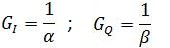
were GI and GQ are the I and Q channel gain- adjustment factors respectively
The essence of this paper is to develop an idea to digitally predistort the signal to be transmitted so that the nonlinearity effect that might appear later on could be effectively compensated. However, the signal processing efficiency is not discussed so far, but in order to practically implement such an architecture, the signal processing methodology and speed need to be considered as well. The early prototyping venture should be mindful of the fact that despite the theoretical understanding and predictions that are taken care of in the presented architecture, there might be some other practical issues which also needs to be addressed in the design of the calibration process.
The non-ideal response of the transmitter is defined by several parameters, such as phase error, IQ mismatch, carrier leakage, AM/AM and AM/PM distortion from the PA, and gain variance of the power amplifier. The functional model of the distortion of the otherwise perfect transmitter components is a useful tool to understand the non-ideal response, and to achieve appropriate compensation method against distortion.
In the theoretical analysis, part of the transmitter, and mathematical descriptions of both ideal and non-ideal components have been analyzed in this paper. Any linearization scheme that might be deployed should consider the mathematical distortion model of different components of the transmitter. The calibration part presented is the most important element of the proposed Software Defined Radio (SDR). The transmitter complexity to achieve the goal of the SDR is a matter of flexible design concept.