Figure1. Communication Block Diagram
This paper, presents a method to describe all modulation techniques such as BPSK, ASK, FSK, QPSK, OOK. These are compared based on bandwidth requirement, power efficiency, transmission capacity and bit error probability. The modulators are the basic requirement of optical communication systems and they have been designed to reduce the channel distortion, and hence many types of modulation techniques have been proposed here. This paper, mainly focuses on the hardware realization of such several modulation schemes with a minimum area strategy for the universal mobile telecommunication system when it comes to power and error performance. Here MATLAB software is used for simulation and result analysis.
The use of infrared frequencies for short-range wireless communication have received extensive interest over the past decade, and many potential applications for this technology have been suggested for various configurations which may be used by an indoor optical wireless communication system. The diffuse configuration is more desirable from a user's point of view, since no alignment is required prior to use, and the system does not require a line of sight path for transmission. Diffuse systems rely on reflections from ceilings, walls, and reflecting objects within the room to provide coverage, and are susceptible to ambient light noise, high signal attenuation and inter-symbol interference caused by multipath propagation [1]. Communication may be intentional or unintentional, might involve standard or unconventional signals, might take linguistic or non-linguistic forms, and should occur through spoken or different modes. Communication needs a sender, a message, and a recipient, and though the receiver does not need to be alert to the sender's intent to speak at the time of communication. Communication will occur across large distances in time and area [2]. In Digital modulation, the digital information is transferred as a series of ones (1) and zeros(0) as input signals and amplitude. Frequency or phase of carrier signal is shifted according to digital input, so this technique is also known as shift keying. But in digital modulation, instead of varying the amplitude or the frequency of the carrier signal, it is preferred to vary the phase because it offers better protection in transmitting signals [3]. Usually, diffuse transceivers require the use of large area photo detectors.
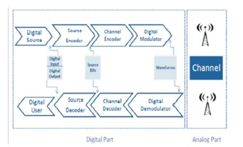
Figure 1 shows the block diagram of communication system. However, the high capacitance associated with large-area photodetectors limits the receiver bandwidth; hence, the spectral efficiency of the modulation scheme is also an important consideration. There are several modulations and/or encoding schemes that are suitable for optical wireless systems and the following sections represent outlined comparison between some of them [1].
Figure1. Communication Block Diagram
After the conversion of an analog signal to digital by sampling, different type of digital modulation schemes can be applied by the variation of different parameter of the carrier signal. Frequency variation gives BFSK and the phase variation gives BPSK. Also, sometimes a combinational variation of the parameters is done to generate the hybrid modulation technique viz. a combinational variation of Amplitude and Phase Shift Keying (APSK). Many more digital modulation techniques are available and can be designed depending upon the type of signal and the application. These digital modulation techniques can be classified basically either on the basis of their detection characteristics or in terms of their bandwidth compaction characteristics [4].
The binary phase shift keyed modulator is the simplest of app PSK modulators since, it has only two output phase states at the same frequency, but separated by 180º. The general form for the BPSK signals are according to (1), where fc is the frequency of the carrier [5]. If 1 is transmitted, the modulated signal remains the same as the carrier, with 0º initial phase, but if “0” is transmitted, the modulated signal would change by 180º binary sequence which is multiplied with the sine wave generated by the oscillator to get the BPSK modulated signal. The carrier is recovered by the carrier recovery circuit. The BPSK modulated signal is multiplied with the sine wave generated by the carrier recovery circuit and passed through the integrator and the decision device to detect the original modulated signal. If the second input is logic 0 then sine wave is the output of the switch and if the input is logic1 then output is 180 degrees .
Figures 2(a) and 2(b) show the modulation waveform [6] of BPSK and constellation diagram. The digital communication is the transmission of information in digital form from source to destination. In the analysis and design of communication system, the characteristics of the channel affect the design of the basic building blocks.
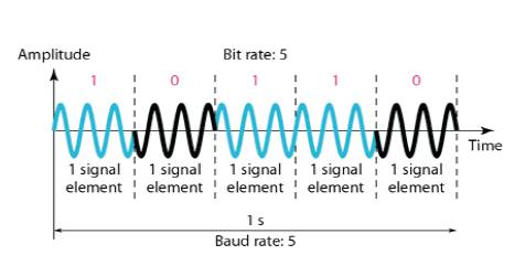
Figure 2. (a) BPSK Modulation waveform
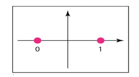
Figure 2. (b) Constellation diagram
In ASK modulator the level of amplitude can be used to represent binary logic 0s and 1s. We can think of carrier signal as an ON or OFF Switch. In modulated signal logic 0 is represented by the absence of carrier, thus giving OFF/ON keying operation.
Figure 3 shows the general working diagram of Amplitude Shift Keying (ASK). At receiver side ASK modulated signal is multiplied by the carrier signal which is generated from the carrier generator output. The Multiplier consists of higher frequency and lower frequency components and this output is integrated by integrator block and passed to the Comparator block. Comparator blocks recover digital data by comparing threshold values with integrated signal [7].
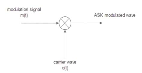
Figure 3. ASK modulation
Frequency Shift Keying (FSK) carries the information signal by representing the transmitter alphabet with M symbols using carriers with M discrete frequencies. In general it is called M-array FSK. When M is 2 then it is called Binary FSK with two carriers, usually termed as the mark and space frequencies. In FSK, two carriers f1, f2 are used whose frequencies will differentiate between logic 1 and logic 0. Single carrier can also be used for optimized system. In the Simulink/system generator environment, we have to configure each block with their corresponding parameters to get the accurate output [8].
QPSK (Quadrature Phase Shift Keying) is one of the modulation schemes used in wireless communication system due to its ability to transmit twice the data rate for a given bandwidth. QPSK can achieve twice the spectral efficiency with same energy efficiency. QPSK modulation is a type of Phase Shift Keying (PSK) in which carrier is modulated with two data bits from the data stream simultaneously. This results in one out of four possible carrier phase states i.e. 0°, 90°, 180° and 270°[11]. But the exact phase retrieval becomes a very important factor for the receiver design considerations, failing which can give rise to erroneous detection of the signal. This factor increases the receiver design complexities. To compensate for these problems, normally the idea of pulse shaping the carrier modulated signal is employed with the Root Raised Cosine Pulse shaping for achieving better performances which however which has a limitation that the constant envelope property of the signal is lost [4]. The QPSK can be used either to double the data rate compared with a BPSK system while maintaining the same bandwidth of the signal, or to maintain the datarate of BPSK but halving the bandwidth needed. In this latter case, the Bit Error Rate of QPSK is exactly the same as the BER of BPSK. The binary sequence is separated into an odd-bit sequence I and an even-bit-sequence Q with thehelp of the sample and hold block. The Sample and Hold block acquires the input when it receives a trigger event at the trigger port. The block then holds the output at the acquired input value until the next triggering event occurs [3].
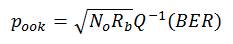
Modulation is the process by which a data is transformed into an analog waveform that is suitable for transmission [10]. To realize an easy transceiver architecture with noncoherent modulation, the authors resort to On-Off Keying (OOK), which is the simplest amplitude-shift keying. It is well known that the OOK power spectral density is a sine square function with main lobe width around the carrier. Similar to Frequency Shift Keying (FSK) and Binary Phase- Shift Keying (BPSK), OOK supports data rate up to half the available bandwidth. The error probability (or Bit Error Rate, BER) of a non-coherent OOK demodulation is given by [9].
Where Eb and No denote the average bit energy and noise power spectral density, respectively. The error rate of OOK demodulation is very close to that of FSK, but is inferior to that of BPSK. However, to avoid the complicated carrier recovery circuit, the authors chose OOK for such a shortdistance system. Note that none of the published 60-GHz solutions utilizing BPSK, QPSK can discard the baseband circuitry.
The analysis and output of BPSK, ASK, FSK, QPSK, OOK are shown below. This analysis are done by using matlab software.
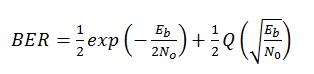
The BPSK modulator in simulink consists of two sine wave generator, a binary data source, a switch and the scope to view the results at various stages of the circuit. The output of product is then passed through the low Pass filter which removes the noise from the signal. The output of the transfer function is then compared with the constant by the relational operator. If the value of the output is greater than 0 then output is 1 and if the Value is less than 0 then output is 1. Figure 4 shows theoutput waveform of BPSK. According to the second input, first and third inputs are controlled
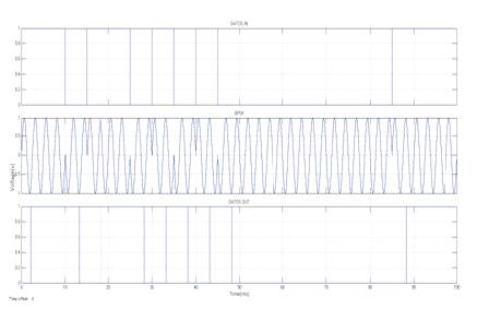
Figure 4. Output waveform of BPSK
If the second input is logic 0, then sine wave is the output of the switch and if the input is logic1 then output is 180 degrees phase shifted sine wave. The output of the switch produces the BPSK modulated signal.
Figure 5 shows the ASK(Amplitude Shift Keying) output waveform and shows clearly the variation of the signal. In ASK modulator, level of amplitude can be used to represent binary logic 0s and 1s and carrier signal as an ON or OFF Switch. In modulated signal logic 0 is represented by the absence of carrier.
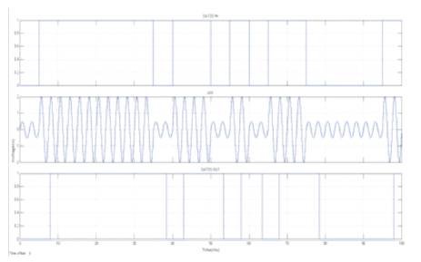
Figure 5. Output waveform of ASK
Figure 6 shows the output analysis waveform of Frequency Shift Keying. Let there be a frequency shift by ohms. Here the two frequencies are used to carry the symbol or binary bit. Consider here that one frequency carries binary bit 1 and second frequency carries the symbol 0. Input bits in form of 0 and 1 carry both the frequencies without any interference and get modulated. Carrier signal carry the signals in phase. In Frequency Shift keying, the frequency of carrier is shifted according to the binary symbol [7]. The phase of carrier is unaffected. After the modulation of signals, we require the original signals so that, demodulate the signal can be demodulated.
Figure 6. Output waveform of FSK
In a digital transmission, BER is the percentage of bits with errors divided by the total number of bits that have been transmitted, received or processed over a given time period [12]. The switch blocks will choose between the first or third output depending on the value of the second input. In the case of the I-channel, if the second input is 1, the output value will be cosine, but if the second input is 0, the output will be cosine and for the Q-channel, if the second input is 1, the output value will be sine, but if the second input is 0, the output will be –sine. The sum block combines the two modulated signals into the QPSK signal. Figure 7 illustrates the output waveform of QPSK. The output waveform shows information bits in 1 axis after thatreception of bits during demodulation process. Last and very important topic of QPSK modulated waveform is shown in last block according with its theory.
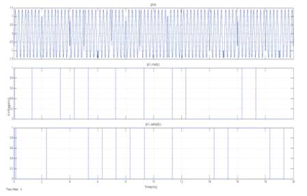
Figure 7. Output waveform of QPSK
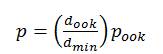
Figure 8 shows the output waveform of OOK.We will use OOK as a benchmark to compare the power efficiencies of various modulation schemes. The power required by OOK to achieve a given BER is:
The power required by any other modulation scheme to achieve the same BER is approximately
The output variation of OOK modulation is shown in Figure 7.
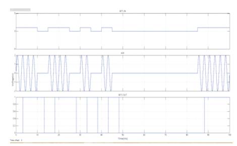
Figure 8. Output waveform of OOK
The implementation of digital modulation techniques BPSK, ASK, FSK, QPSK, OOK for optical communications was done by using MATLAB. If the parameter of the system changes it produces different operating signal. The modulation techniques are the basic requirement of optical communication systems and are designed to reduce the channel distortion. Hence many types of modulation techniques have been proposed and implemented here. These different modulation and demodulation properties vary between themselves. These modulators are used for variety of applications depending upon the requirements and applications as and where needed.