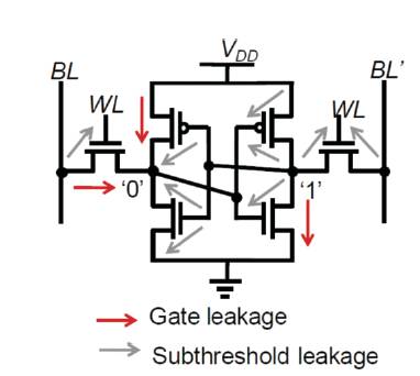
Figure 1. Static power dissipation components in 6T SRAM
This paper presents a brief review on different types of Tunnel Static Random Access Memory that has been proposed for low power applications. Many authors and researchers have worked on tunnel SRAM, RTD/HFET low standby power, SRAM gain, cell and Bistable Body Tunnel SRAM and demonstrated the accomplished improvements in power dissipation and performance compared with previous designs for low-power memory operation. It broadly relates to SRAM cell employing a Tunnel Switched Diode (TSD) that acts as the storage medium and is controlled by a pass transistor.
Historically, Complementary Metal Oxide Semiconductor (CMOS) digital circuits are the enabling technology for the modern information age. Because of its main characterises i.e. low power consumption, large noise margins and high stability. CMOS integrated circuits have been broadly used to develop RAM chips. As memory cells started to dominate chip area in high performance applications, SRAM has become the focus of technology scaling. Static Random Access Memory (SRAM) is being used with increasing frequency in a wide variety of applications requiring temporary data storage. The trend toward higher density and higher performance memories has resulted in a number of improvements in SRAM architecture. For example, BJT based single transistor, and diode-based single transistor SRAM cells are representative of two new memory devices. However, these devices have certain advantages and disadvantages [11]. For example, BJT (Bipolar Junction Transistor) based SRAMs suffer from reliability problems and they are complex and large in size, while diode based SRAMs are not suitable for being manufactured in CMOS technology processes. Conventional SRAM cells generally operate at relatively high cell current levels, but take up a relatively large area because of the need for using as many as 10 transistors per cell. The basic need is an improved SRAM cell, that is relatively small in physical area, thus allowing high memory array cell density, while also providing for power dissipation that is required in high performance and low power applications.
Several types of SRAM cell configurations have been proposed for low power applications. Some of the other new SRAM cell configurations exploit bipolar base current reversal. Examples of such configurations can be observed in Koji Sakui et al [1], U.S. Pat. No.5, 594,683 which discuss the new Static Memory Cell Based on Reverse Base Current (RBC) Effect of Bipolar Transistors. These and other new SRAM cell configurations help in achieving smaller cell size and lower power dissipation of the SRAM memory cell [12].
Another alternative configuration is proposed by Van der Wagt et al [2], RTD/HFET Low Standby Power SRAM Gain Cell. This configuration uses only two tunnel diodes and a single FET, but however suffers from relatively high standby power consumption (approximately 50 nano watts per cell). The high standby power consumption is partially due to the fact that the cell described here is fabricated using III-V technology (integrated circuits fabricated on substrates such as Ga-As comprising combinations of elements from groups III and V of the periodic table).
The objective of this paper is to discuss technologies that reduce power dissipation and reduce the chip area. Conventionally, 6T SRAM cell configuration was used for the storage purpose and it has several advantages and disadvantages that are discussed further in this paper.
Conventionally six transistor (6T) SRAM cell configuration uses an ultra-low power supply but it has high power dissipation so this cell shows poor stability at very small features sizes. It consists of six transistors configured as cross-coupled inverters to form a flip-flop as described in “CMOS Technology for 1.8V and Beyond,” by Jack Y. C. Sun [3]. Since the inverters are cross coupled, excellent state stability results even if each single inverter is highly asymmetric in its pull-down and pull-up output drive capability. The drive to achieve reductions in cell size and chip area have led to the use of vertical transistors, but through this technology, which is quite more complicated and hence more costly, the feature size cannot be reduced as much as is required. Thus, although absolute SRAM cell size can be improved with reductions in featured size corresponding to advances in lithography technology, further reductions in SRAM cell size require changes in cell configuration. As stated herein, cell configuration refers to the components that are used i.e. transistors, diodes of the cell and their interconnection. Configuration has a different meaning from structure. Structure, as stated herein, refers to the physical connections of the fabricated cell.
Figure 1 [13] shows the different components that result in the static power dissipation in a 6T SRAM cell. Since the transistor gate leakage is higher than the subthreshold leakage in OFF state, the static power dissipation is dominated by the subthreshold current of the transistor. So, 6T SRAM cell suffers from a very important drawback, that is, high power consumption. It is the amount of the power that is consumed by a memory cell when neither write nor read operation is performed by the cell.
Figure 1. Static power dissipation components in 6T SRAM
To solve the problem of subthreshold leakage, researchers developed many other structures that include bistable behavior of tunnel diode and many more. Some of them are discussed in this paper.
Other new structures utilized latchup as a mechanism of cell operation. Latching mechanism uses tunnel diode as a latching circuit and the switching of tunnel diode is controlled by a pass transistor.
The Tunneling based SRAM consists of a single pass transistor and a pair of low-power RTD's [see Figure 2(b)] [10]. RTD's are quantum devices that operate in Negative Differential Resistance (NDR) and can be used over the commercial IC temperature ranges, exhibit excellent reliability, and naturally store 1 bit in a latch constructed from only two devices. As negative differential resistance phenomena are able to exhibit two stable voltage states it is suitable for the memory operations.
The first tunnel diode SRAM cell was proposed by Goto et al. [4]-[5], consisting of only one FET and two tunneling devices [see Figure 2(a)]. The device resembles a conventional DRAM cell which consists of a transistor and a capacitor [7]. Here, in this device, in place of capacitor, a pair of resonant tunnel diodes are used for a latching mechanism and data will be held in the pair of these resonant tunnel diodes.
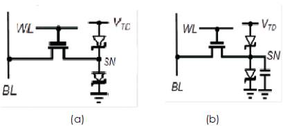
Figure 2(a). Tunnel device Goto SRAM cell [4]. (b) TSRAM cell. VTD is a positive supply voltage. Ideally, the TSRAM cell capacitance is realized as part of the NDR devices
A load-line diagram shows two stable points close to the supply levels. As in the conventional SRAM cell of Figure 3, large restoring currents oppose perturbations around these points. For LSI memories most important features are small chip area, sufficient current drive, very small standby power, and a large amount of signal to noise margin. To achieve LSI-compatible standby power with a Goto SRAM cell [4], a valley current density below 1 A/cm2 is required. On the other hand, fast SRAM sensing requires peak current densities over 10 A/cm2 [6]. Thus, Goto cell would require an RTD which has PVCR greater than 10. Since RTD PVCR's are only of the order of ten and are not expected to increase greatly, Goto SRAM cells are incompatible with LSI.
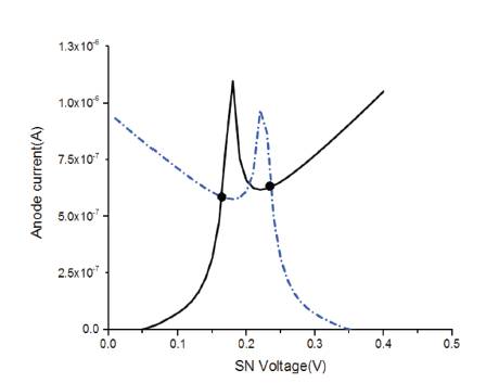
Figure 3. Load-Line diagram for two series connected Tunnel Diode. Dots in load-line diagrams indicate stable points
J. P. A. Van der wagt et al. [8] proposed a new high-density low-power circuit approach for implementing Static Random Access Memory (SRAM) using low current density Resonant Tunneling Diodes (RTD's). A 50-nW standby power compound semiconductor TSRAM cell is demonstrated by combining ultralow current-density Resonant-Tunneling Diodes (RTD's) and Heterostructure Field Effect Transistors (HFET's) in one integrated process on an InP substrate [10]. This power represents over two orders of magnitude improvement over previous III–V static memory cells. By increasing the number of vertically integrated RTD's we obtain a 100 nW tri-state memory cell [9]. The cell concept applies to any material system in which low current-density negative differential resistance devices are available. Experimental results for a compound semiconductor, 1-bit 50-nW TSRAM gain cell using low current density (1 A/cm2 ) RTD's and low-leakage heterostructure field effect transistors are presented. The authors describe a one-transistor TSRAM cell which could convert silicon Dynamic RAM (DRAM) to ultradense SRAM if an ultralow current density (1 A/cm2 ) silicon bistable device is developed. Write and read operations of this tunnel static RAM cell is quite the same as of the 1T dynamic memory-cells. During a read operation, the storage node shares charge with the bit-line which is connected to the drain terminal of the pass transistor and write operation is performed by the help of the gate terminal.
Figure 4 [2] shows a gain cell configuration that is used for the tunnel SRAM. A III–V memory cell for LSI should ideally provide both low power data storage and high current drive access. By connecting a low-current RTD latch to the SN of a dynamic gain cell, a Tunneling-based SRAM (TSRAM) cell is obtained. It is more compact than the standard 6T cell and has demonstrated a record low standby power, with another order of magnitude reduction expected from downscaling [2].
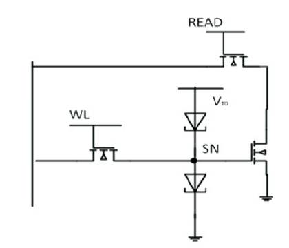
Figure 4. Gain cell configuration for tunnel SRAM
In bistable-body TSRAM cell charge is stored in the pass transistor body and that is held by the latching circuit i.e. TD pair. In this approach body charge of the transistor shifts the threshold voltage and this is sensed by the resulting change in the MOSFET drain current [13]- [14].The ability to sense this change in the drain current of the transistor forms the basis for reading operation of the logic state of the cell. In the presence of transistor leakage, the static current through the TDs ensures that the SN potential remains latched to either near 0 V or near the TD bias voltage, VID .
Figure 5 [13] represents the bistable body tunnel SRAM that consists of the two tunnel diodes and a pass transistor. The power dissipation in the body-biased TSRAM cell is lower than in previously investigated TSRAM because the body current of the transistor has orders of magnitude lower than the subthreshold transistor leakage current and allows orders-of-magnitude-lower-leakage TD to be incorporated [15]. In order for the series TD pair to maintain the state, it is necessary that the peak current in the TD be higher than the total leakage due to all the static leakage current paths from the SN. Since the SN is connected to the body, the leakage current paths from the SN nodes are given by the reverse-biased body-to-source current, the body-to-drain current, and the body-to-gate tunneling current. The total static body leakage current is seven orders of magnitude lower than the subthreshold leakage current of the pass transistor [16]. The static leakage of the 6T SRAM cell is calculated with the help of the subthreshold leakage current of the transistor. In the bistable-body TSRAM the static leakage is dictated by the body leakage current [17]. For this reason, the static current of the bistable-body TSRAM cell can be more than seven orders of magnitude lower than the static current in a 6T SRAM cell. So, it can be easily concluded that by using the bistable-body Tunnel SRAM the power dissipation can be reduced.
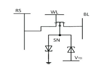
Figure 5. Body Biased Tunnel SRAM cell consists of pass transistor and dual tunnel diode as a bistable circuit to store the data .
In this paper comprehensive look of different SRAM memory cell that are 6T SRAM, Tunnel SRAM and Bistable Body Tunnel SRAM has been studied. The merits and demerits of the different SRAM memory cells are discussed. The performance analysis of different parameters like subthreshold leakage current, total power dissipation and chip area were also studied. The Bistable Body TSRAM is promising cell for low power dissipation and for reduced chip area. The cell uses one transistor and two tunnel diodes is a high speed, low power static memory cell, offering over four orders of magnitude reduction in static power compared to the 6T SRAM and other Tunnel SRAM structure. The success of these SRAM memory cell in terms of power dissipation and chip area will help in improving the performance of digital circuits and memory devices.
This work has been supported by the AICTE under Research Promotion Scheme (RPS-60) for developing Tunneling based SRAM structure in VLSI lab of ECE department MMMUT, Gorakhpur.