(1)
Power Integrity (PI) is becoming increasingly important in today's high-speed digital I/O interfaces. Power integrity for I/O interfaces is related to the voltage variations in the power/ground network due to the noise. The power/ground noise causes various problems in high-speed systems, such as logic failure, EMI, timing delay, and jitter. For the Power Integrity analysis of the I/O padring of the chip, it is very important to quickly calculate I/O current consumption at the early stage of the project, without running extensive time-consuming spice simulations of entire I/O bank. PI analysis needs both I/O padring and PCBdata, and simulation tool considers them simultaneously [5],[6],[7],[10]. Two useful formulas are given in this article and explained below that can easily allow to estimate average and maximum IO current consumption, using example of i.MX6 series applications processors of Freescale Semiconductor, Inc. Resulting numbers correlate well with real I/O circuit spice simulation data.
The power integrity has several impacts to the I/O signaling as follows:
Simply, average current of I/O cell defines power consumption in its operation mode and maximum current means maximum transient peak current. The power supply capability requirements of I/O bank of the chip mainly depend on the average current value, but it is also very important to calculate the maximum current as well. System reliability design needs to assess transient current of IO, and Power Integrity (PI) simulation tool may be used for current consumption analysis. Faster and reliable analysis at the early stage of the project is a key benefit to save design cycle time.
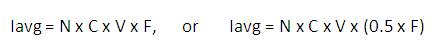
According to i.MX6 series applications processors Datasheet[3], Freescale provides a calculation formula for I/O bank average current consumption as below:
Where,
N -Number of I/O bank pins supplied by the same power bus.
C -Equivalent external c
apacitive load.
V -I/O bank voltage.
F - Clock change rate for the particular I/O bank, or I/O interface.
(0.5 xF)- Data change rate. Up to 0.5 of the clock rate (F)
In equation (1), Iavg is in Amps, C in Farads, V in Volts, and F in Hertz.
The key parameter is C under certain F. Max Load capacitance depends on I/O interface type (industrial Spec requirement) or on I/O interface operating frequency (maximum possible driving capability of the I/O). Actual Load capacitance can be considered as following:
C = Cio (parasitic capacitance of I/O pad and package) + Cload (transimission line (T-line) and connected pin capacitance).
Cio can be extracted from IBIS model. Typical equivalent capacitance of 50 ohm T-line is around 3 pF/inch (which should not be taken into account for this preliminary assessment, but is implemented in spice model of T-line to be accounted in real simulations).
Let's discuss how to estimate Iavg of I/O bank using a real application case.
There are total 29 GPIO pins used in i.MX6 platform display interface bank on NVCC_LCD power domain, as presented in Figure 1.
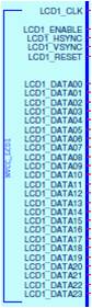
Figure 1. i.MX 6 display interface GPIO bank.
According to I/O library datasheet, GPIO can drive 30pF maximum output load at ~100MHz frequency, and 15pF maximum load at ~200MHz frequency. That max drive capability numbers of I/O give us an upper limitation of frequency and load capacitance.
Consider 1080P@60Hz @ 3.3V display application case, clock rate is around 170MHz.
Then at these conditions, we can calculate the max possible average current per one data pin of the bank:
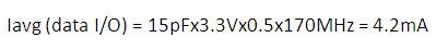
For the clock pin:
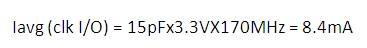
The above equations are max possible average current of GPIO under certain frequency, when signal is toggling twice per cycle. In spice simulations, the maximum conditions for the current are: best process case, I/O VDD max, and 125C temp.
Other 3 sync/enable signals of display interface bank have lower data rate. Let's estimate 1/3 data current for each of them. Reset signal is static. Then
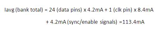
Proper current estimation is always preferred, because current over estimation is not good for a product, since it means power bus structure over design.
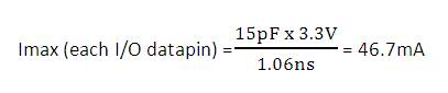
For the maximum current calculation, the following known formula can be used [1], [2]:

Where,
n is the number of loads.
C is the capacitance of load.
V is the power supply voltage.
tr is the rise time of output waveform.
Similar to consideration in the above section, the authors found in the AC parameters of I/O from the I.MX6 datasheet in Table 1.
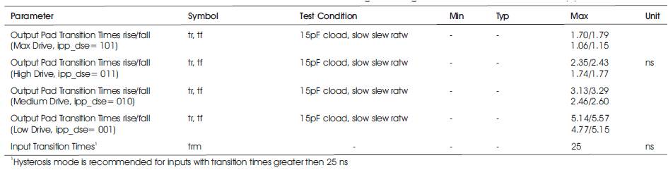
Table 1. General Purpose I/O AC Parameter 3.3 V Mode
Note: Please refer to reference manual of i.MX6 (Reference 3) series applications processors for the meanings of IO configuration pins.
Under fast slew rate, ipp_dse=101 (max drive strength),and 15pF Cloadcondition, with trise = 1.06ns,
But for the same LCD display interface use case, we cannot use the data of each pin multiplied by total pin numbers in the bank. For proper estimation, the authors checked the real data pattern.
We can check transfer timing sequence in a LCD spec, but not all the pins will change status at the same time. So we can estimate that only 24 bit data lines will work at the same time. Then the authors calculated the total maximum current on LCD power rail:
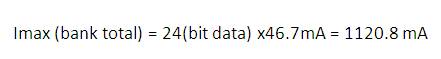
The resulting number is quite big, more than 1A,but this is usual transient peak current value under heavy use case for the above application. We should consider it for the maximum PI (Power Integrity) performance.
For the Power Integrity analysis of the I/O padring, and particular I/O banks of the chip, quick I/O interfaces current consumption estimation is very important on the early stages of the chip design, and SOC teams always request this data from I/O design teams in advance, before final I/O circuit and layout is developed. Power Integrity (PI) simulation tool may be used for further current consumption analysis. Such faster and reliable analysis at the early stage of the project is a key benefit for design efficiency. Two useful formulas are given in the article with explanation on how they can be easily used to estimate average and maximum I/O current consumption, using example of i.MX 6 series applications processors of Freescale Semiconductor, Inc. Practical analysis of selected I/O bank average and maximum current consumption was demonstrated in this article. The formulas give pretty accurate results, the resulting numbers correlate well with real developed I/O circuit and post-layout spice simulation data.