(1)
Scaling of the CMOS [Complementary Metal Oxide Semiconductor] technology associated with gate oxide thickness has become a major barrier for the design of circuit in nanoscale Static Random Access Memory (SRAM), especially in lower voltages. The operation of SRAM arrays are critical in reducing the power consumption. The Gate Oxide Breakdown caused by excessive electric field in the gate oxide causes increased vulnerability of the circuit performance, during breakdown. The devices are characterized by increased minimum voltage due to increase the static write failure as the voltage decreases. The design circuits were schematized using the DSCH2 schematic design tool, and their layouts were generated with the Micro wind 2 VLSI layout CAD tool. The proposed structures are simulated using Xilinx ISE design suite.
Device length scaling has been accompanied by a continuous reduction in gate-oxide thickness with the aim of maintaining acceptable device performance [1]. Reliability margins of these aggressively scaled devices have been reduced. This problem has been somewhat alleviated by the introduction of high-dielectric gate stacks which have shown improvement in terms of reliability, but as the results indicate, gate oxide breakdown can still have a significant impact in determining the lifetime of a device.
Throughout the lifetime of a device, various oxide defects, called oxide traps, are formed on the oxide. As their density increases, the traps start to overlap, eventually reaching a “critical defect density” where a continuous defect path is formed through the oxide. This results in an increase in the gate leakage current and is known as soft breakdown (SBD).
SBD may not coincide with device failure. Although operational degradation is seen, device switching characteristics and logical functionality may be maintained even after SBD leads to a significant increase in device reliability margins for digital circuits.
To understand the impact of Gate Oxide Breakdown (GOBD) on a functional block, it is imperative to understand the circuit level implications of SBD. A post-SBD transistor may show gate currents that are the orders of magnitude higher than nominal values. When time gate leakage further increases, the device loses its transistor characteristics and enters Hard Breakdown (HDB). At the circuit level, this region of gradual decay between SBD and HBD leads to weakening logic voltages, degrading drive currents, and increasing logic delays. Predicting device failure is possible if this gradual degradation can be monitored and routed to HBD[2]. The purpose of this project is to rigorously define the HBD point of an SRAM cell based on its required performances and to provide a method to monitor device degradation so that impending HBD can be detected prior to its occurrence.
In this work, the authors start off with an exhaustive analysis of the effect of GOBD on the DC margins of a 6T SRAM cell. The authors also show that GOBD can cause timing failures in SRAM cells because of access time degradation, leading to frequency dependent failure probabilities. From the combination of these results, the authors formalize a definition for the HBD point for a cell (HBDcell).
The authors have oriented an on-chip Process, Voltage, and Temperature (PVT) tolerant monitoring scheme. The monitoring scheme involves checking all cells in an SRAM word-by-word and has a trigger point associated with the HBD point. Hence, any cell approaching HBD can be detected. The oriented scheme does not involve taking the memory offline for testing purposes, as testing can be done during normal system operation without incurring any penalty.
A conventional SRAM cell consists of three types of transistors (latch PMOS, latch NMOS and access NMOS), and each one is critical to correct memory operation.
Figure 1 shows the design of a conventional 6T SRAM cell. Due to the different roles each play during read/write/retention[5], the gate size and the amount of time the dielectric is under stress varies significantly among the three types of transistors.
It has been shown that Weibull failure rate distributions provide a good fit for the rate of dielectric breakdown of both PMOS and NMOS transistors.
Where,
P(tfail) - Probability of failure
η, β - Two parameters that characterize the Weibull distribution
Weibull distribution equation (1) explains the probability that failure will occur before time tfail η and β and are the two parameters that characterize the Weibull distribution. Interpolating lifetimes from reliability stress tests to normal operating conditions are usually done using exponential or power law models with the latter being the accepted model for gate dielectrics, since the former violates the Weibull scaling law.
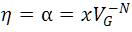
The power law relates, the power law exponent, to the characteristic lifetime and the operating voltage as follows:
Where,
α - Voltage dependent constant
VG-N - Operating Voltage
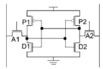
Figure 1. Conventional 6-T SRAM cell
Although changes in threshold voltage and device Trans conductance have also been observed as a result of a degrading gate dielectric, GOBD is generally modeled as an increase in gate leakage current. The leakage path could appear between the gate and the source/drain region or between the gate and substrate. Experimental results have shown that gate-to-substrate leakage usually has a minimal effect on circuit performance compared to gate-to-source/drain leakage [3]. Therefore, GOBD resulting in gate-to-substrate shorts has been ignored in this work. Moreover, it shows that failure probabilities of PMOS(Positive Channel Metal Oxide Semiconductor) and NMOS(Negative Channel Metal Oxide Semiconductor) devices in the latch are comparable at operating conditions, therefore the effects of a breakdown event in the oxide of both type of devices are analyzed.
Figure 2 shows the PMOS gate leakage models used for the analysis and how these models fit into the SRAM cell. The model was used to model the gate-to-source leakage path, while the model was used to model the gate-to-drain leakage path.
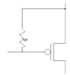
Figure 2. Gate-to-source leakage model
The gate-to-source leakage path results in leakage to the positive supply and ground for the NMOS and PMOS devices, respectively. The gate-to-drain leakage path results in leakage between the two sides of the cell, the one storing a logic “0” and the one storing a logic “1”.
Generally, the analysis of GOBD in SRAM cells has been done using the models shown in Figure 3 and 4. But these models do not account for the change in drive current caused by GOBD, and hence cannot be used to estimate the access time shifts in the SRAM cells. The degradation in device drive current has previously been modeled and have used the same model to study the effect of GOBD on cell access times using the Rpoly/metal resistance along with the leakage models[4].
Figure 4 shows the possible leakage paths in an SRAM cell. Here Rpoly/metal is present irrespective of whether a breakdown event has occurred. NMOS-Rgs , PMOS-Rgs , and Rgd represent the possible leakage paths through the dielectric. The paths through NMOS-Rgs and PMOS-Rgs constitute leakage to the positive supply and ground, and the path through Rgd constitutes leakage between the two storage nodes of the cell.
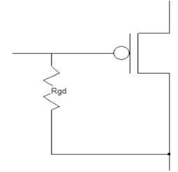
Figure 3. Gate-to-drain leakage model
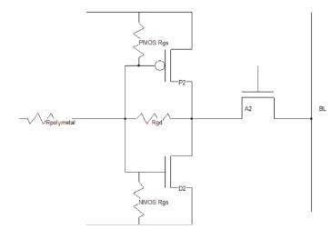
Figure 4. Leakage paths in an SRAM cell
The aim is to monitor NMOS and PMOS cell current. First consider the PMOS cell current. It is difficult to access the PMOS current during either the read or write operations. During the write operation, initially the current in the bit-line next to the node that stores a “1” is dominated by the PMOS device current. However, as the voltage falls below the tripping point of the inverter, this PMOS turns off, and the remaining current in the bit-line is from the NMOS device.
Hence, the author cannot separate the current due to the two devices. On the other hand, the read operation does not involve the PMOS device at all.
In order to access the current in the PMOS devices, the cell state in Figure 5 is proposed. As shown in the figure, to put a cell in this state, both bit-lines are forced to zero, in the 1st clock cycle. Writability of the cell insures that the internal nodes of the cell, V1 and V2, are both close to zero. When the internal nodes are both close to zero, the NMOS latch transistors D1 and D2 are turned off and the PMOS latch transistors P1 and P2 are turned on. The current from the PMOS latch transistors P1 and P2 flows through the access transistors A1 and A2 onto the bit-lines. The resulting bit-line currents are labeled I1 and I2 in Figure 6.
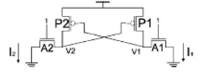
Figure.5 SRAM cell state for PMOS testability
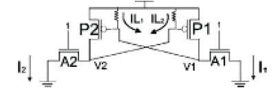
Figure 6. SRAM cell state in test mode, illustrating the PMOS gate-to- Source leakage currents
During PMOS gate-to-source breakdown, the leakage current through P2 supplements I2 , and the leakage current through P1 supplements l1 . These leakage currents are illustrated in Figure 6. The currents I1 and I2 flow through the bit-lines to ground during this first clock cycle.
The monitoring method requires a few additional control signals for testing and involves modifications to the read/ write and the decoding circuitry. In addition, the implementation requires IP and IR blocks, and possibly a register file. The register file is for temporary storage of bits for the cells being tested, since the testing process is destructive to data[6].
The register file is for temporary storage of bits for the cells being tested, since the testing process is destructive to data.
Figure 7 shows the General Structure of an array-based memory system with the DFT, and the extra storage can be discarded if the test is run when the SRAM is not storing any useful information, e.g., at system startup. Absolutely no modifications were made to the memory array itself [11]. Therefore, the compactness of the array was not compromised in any way.
The proposed testing process takes four clock cycles to complete and consists of two principle test cycles: T-IR and T-IP. In a single test cycle, the reliability of the oxides of the cells under test, whose number equals the word size (WS), is read by the DFT blocks (IP and IR blocks). Each test checks all latch transistors (PMOS and NMOS) on both sides of the cells that are connected to the same word line.
Figure 8 shows a more detailed view of a single column of the array and the corresponding changes to the peripheral circuitry. The array enters test mode (TM) once the control signal TE is asserted. This initiates the T-IP test cycle. The T-IP control signal deactivates the periodic pre charging of the array, causing the bit-line capacitances (Bit-Cap) to float. The appropriate column is selected by the decoder control signals (S0) [7], while the WL of the appropriate row is asserted high.
T-IP is a pseudo write process. Therefore, the control signal, WE, is asserted, and the array enters write mode. In a normal write operation, the two bit-lines of a column are driven to opposite values. Due to the modifications to the write circuitry, in T-IP, both bit-lines are grounded, hence forcing the internal nodes of the cell being tested to ground during the first clock cycle. Then in the second clock cycle, the bit-lines are allowed to float, and the cell under test starts to charge up the bit-lines.
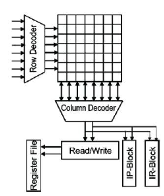
Figure 7. General Structure of an array-based memory system with the DFT Block included
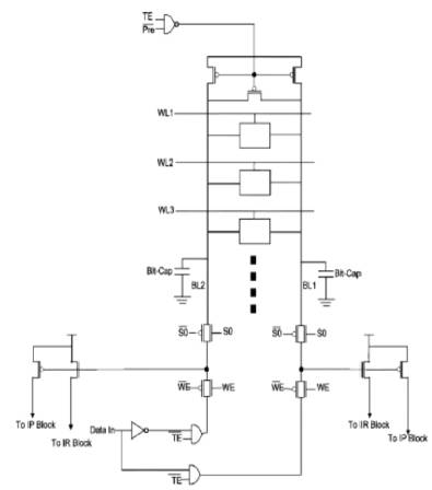
Figure 8. Single column of the memory array with integrated testing system
The T-IP tests the cells under test for a possible breakdown event in the oxide of PMOS devices in the cell. Next, the test cycle enters the T-IR test mode[11]. This mode acts like a normal read access for the array column. It starts off with the bit-lines being pre charged to Vdd by the pre charge circuitry in the fourth clock cycle[7]. The access transistors are turned on. Then the pre charge circuitry deactivates, causing the bit-lines to float. The cell discharges the bit lines.
If the aim of the proposed monitoring method is to implement a high resolution tracker for GOBD for memory cells, then all of the blocks shown in Figure 9.(a), except for the weighted reference generator block in Figure. 9(b), have to be replicated for each bit-line. This enables the tracking of leakage resistance and the identification of failing cells.
Most applications, however, only need to identify cells which may have functional failures in the near future due to GOBD. Once this trigger point is chosen, the implementation of the proposed GOBD testing scheme can be reduced to its low overhead version. This implementation takes into account two conclusions drawn from the preceding results. Firstly, it is highly unlikely that a failure is caused by a leakage event due to the PMOS gate-to-source leakage path and it is experimentally verified. Second, a single trigger point can be chosen that separates fault-free cells and those with gate-to-drain breakdown events affecting nominal operation and those with NMOS gate-to-source breakdown events. Thus, the testing process can be reduced to the IR-Test with a single trigger point. The physical overhead of this scheme is thus greatly reduced and only involves the addition of extra latches/amplification blocks within each sense amplifier.
For better coverage, the IP-Test can be included with the addition of another pair of latches within each sense amplifier or by switching between two trigger points.
If IP-Test is not included, then the memory system does not need to be taken offline for testing purposes, since the IRtest is just a non-destructive read process. With every
Repair rate = # of repaired chips / # of total chips
Normalized repair rate = # of repaired chips / # of repairable chips
The 100% normalized repair rate is called the optimal repair rate. If a memory array is repairable and the number of faults on the memory array is greater than 2rc, there exists at least a must-repair row or column. Where “r” is the number of rows and “c” is number of columns.
Figure 10 shows where the restriction comes from. A wordoriented memory of type B has only spare columns unlike that of type A. Each spare column is selected, when a programmed column address is accessed In the classical spare allocation problem, and the authors consider a bit oriented memory array with spare (repair) rows and spare (repair) columns. Any fault row (column) can be replaced with a spare row (column). A repair solution is a set of at most row addresses and at most column addresses that cover all faults (all faults are on the addresses). If a repair solution exists for a memory array, the memory array is repairable. A repair strategy is a string of the alphabet {“R”, “C”} such that occurs times and C occurs c times cells. Columns associated with the same bit position are clustered together. Read cycle, the active cells can also be tested for possible leakage events to identify the faulty and potentially faulty.
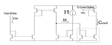
Figure 9(a). Current subtractor & Amplifier
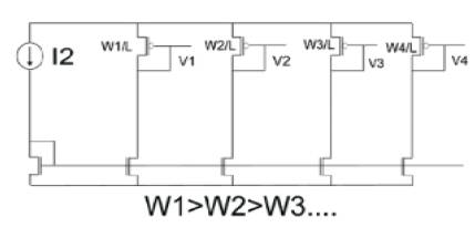
Figure 9(b). Weighted block generator
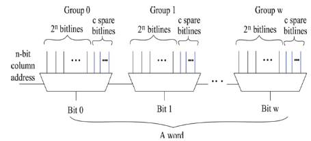
Figure 10. Column circuitry of a word-oriented memory of type A
Figure 11 illustrates the column circuitry of a word-oriented memory of type A. In word-oriented memories, the data in a word is usually not placed in adjacent locations due to several issues such as the coupling effect.
In order to generalize the constraint that arises in type B, the authors define a new term. In a memory, if up to columns out of those associated with a word can be replaced with spare columns, the memory is column-perword replaceable. Thus, memories of type B are 1 column-per-word replaceable.
Once the test is completed (thus the must-repair analysis is done), BIST_Done signal is asserted and the final analysis is started. In the final analysis, the SOLVER module controls the MRA. The operation of the SOLVER and the MRA in the final analysis phase is illustrated in Figure 12.
The SOLVER will generate repair strategies one by one and will check whether each repair strategy can fix all the faults captured in the fault-list. If “R ” and “C ” are mapped to “1” and “0”, respectively, then a repair strategy can be represented by a (r+c) bit word.The Repair Strategy module comprises a -bit register and stores the repair strategy being tested currently [8]. The first repair strategy is generated depending on the numbers of must-repair rows and columns.
After a repair strategy is tested, the state of the MRA should be reverted to that, right after the must-repair analysis, so the values in the L registers are copied to the L_save registers before the final analysis begins. The SOLVER generates the first repair strategy and the MRA reads each fault address in the fault-list in order until there exists no more fault address or the RESTART signal is arrived[9]. The MRA checks if each fault is covered by the current solution, stored in the solution record, and assert R_Covered or C_Covered. If both signals are low, the fault should be covered by a new repair row or column. The SOLVER determines whether a repair row or column is used for the uncovered fault, and asserts R_Insert or C_Insert. If R_Insert (C_Insert) is high, the fault row (column) address is written in the row (column)CAM of the solution record. If the CAM is full, the memory array cannot be repaired by the first repair strategy, and the SOLVER generates the next repair strategy and asserts the RESTART signal. The next repair strategy can be generated directly from the current repair strategy by a combinational circuit called K-subset enumerator, which will be explained in detail in Section V. When the RESTART signal becomes high, the MRA restores the initial state, and the next repair strategy starts being evaluated[10]. In this way, the SOLVER explores the solution space and can find a solution if one exists.
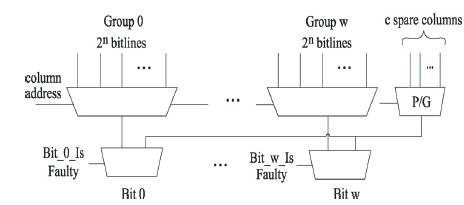
Figure 11. Column circuitry of a word-oriented memory of type B
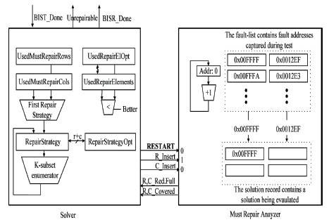
Figure 12. Solver and Must Repair Analyzer Operations
The simulation results are shown using microwind software tool.
Figure 13 shows the design of conventional 6T SRAM cell design. From this design a single bit can be read, write and retrieved.
Figure 14 shows that a single bit is retrieved at NMOS_Qb. Then a general power analysis is done to compare.
The input to the SRAM cell is given as “0”. This SRAM cell is tested for breakdowns in the circuit. The testing SRAM cell is connected to the X-OR gate and a LED. Figure 15 shows that the circuit does not have any breakdowns.
Figure 16 is the simulated output of the design shown in Figure 15. Since the circuit does not have any breakdowns, the simulated output should be “0”. Because for an equal input to the X-OR gate ,the output should be “0”.
Figure 17 shows that the circuit has a breakdown. The testing SRAM cell is connected to an X-OR gate to reveal the breakdown that has been occurred.
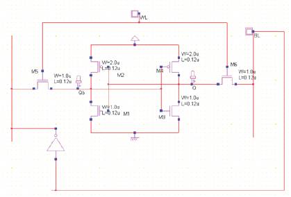
Figure 13. Design of a Conventional SRAM Cell
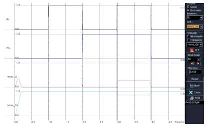
Figure 14. Output of the Conventional 6T SRAM Cell
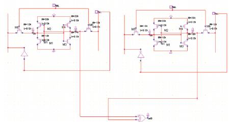
Figure 15. Design of a SRAM Cell without breakdown
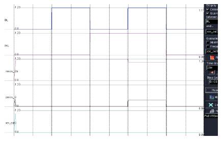
Figure 16. Simulation of an SRAM Cell without Breakdown
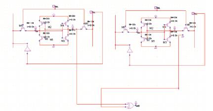
Figure 17. SRAM cell with breakdown
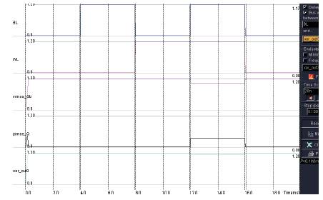
Figure 18. Simulation of an SRAM cell with breakdown
Figure 18 is the simulated output of the design shown in Figure 17. Since the design has a breakdown, the output obtained is “1”. Even though when same inputs are given to the X-OR gate, the output is “1” only. Because the input line that has to be connected with the bit line is grounded.
Figure 19 is the simulated result of a data that has been first WRITE in the memory and then the data has been READ from the same memory. The data simulated is 10101010
Figure 20. shows the simulated result of Must Repair Analyzer .Here the data which has WRITE into the memory is analyzed for whether the cell has to be repaired or not .
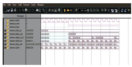
Figure 19. Simulation result Memory Read/Write
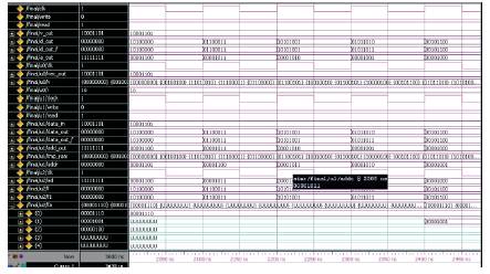
Figure 20. Simulation result of MRA
An exhaustive analysis has been done on the effects of GOBD on SRAM cell performance. The authors have simulated how the DC margins (read, write and retention) are performing in the presence of a breakdown and without a breakdown in an SRAM cell. A hard breakdown point for the cell has been defined (HBDcell) in the simulation. The authors designed a circuit to detect breakdown through placing the cell in a test state and measuring current through the bit-lines. In further the repaired cells are replaced automatically by BISR. The test (single test) takes 600 cycles for four repaired rows and columns.