Figure 1. Logic Structure of Design I
The high speed dual modulus prescaler is one of the important functional blocks in frequency synthesizers. The dual modulus prescaler design is the bottleneck of the synthesizer, as it operates at the highest frequencies and consumes more power than any other circuit blocks of the synthesizer. A dual modulus prescaler (also known as divide-by-N/N+1 counter) normally consists of a divide-by-2/3 prescaler unit followed by several asynchronous divide-by-2 units. Usually, dual modulus prescaler consists of Flip flops and some extra logic implemented using logic gates which determine the terminal count. Here an E-TSPC [Extended True Single Phase Clock] logic based divide-by-2/3 prescaler using pass transistor logic is suitable for low supply voltage (0.9V) and low power applications have been designed and implemented. Here the counting logic and the mode selection control are implemented using a single P-MOS transistor. Thus the critical path is reduced and also increases its working frequency. Simulation results show that, compared with the conventional TSPC [True Single Phase Clock] and E-TSPC based 2/3 prescaler designs as much as 46% in PDP, 24% in operation speed and 44% in area can be achieved by the proposed design. Also the proposed 2/3 prescaler are designed and implemented to design a 32/33 prescaler, 47/48 prescaler and a multimodulus 32/33/47/48 prescaler. The power dissipation of the proposed multimodulus prescaler is lesser than the existing multimodulus prescaler designs shown by the simulation results.
One of the critical functional blocks in frequency synthesizer is the high speed dual modulus prescaler. It operates at the highest frequencies and consumes more power than any other circuit blocks of the frequency synthesizer.
Hence the design of a dual modulus prescaler is so crucial. A dual modulus prescaler usually consists of a divide-by-2/3 prescaler unit followed by several asynchronous divide-by-2 units. For example the topology of a divide-by-8/9 prescaler is implemented in the work done by Xiao Peng Yu [1] which has one 2/3 prescaler unit and two divide-by-2 units. In general a divide-by-N/N+1 counter (otherwise named as prescaler) consists of flip flops and some extra logic implemented using logic gates which determine the terminal count.
Conventional flip flop based N/N+1 counter designs suffer from large load capacitance which limits the maximum operating frequency which in turn increases the power consumption. Therefore, dynamic and sequential circuit techniques[2-4] or clocked logic gates such as, True Single Phase Clocks (TSPC) have to be used to reduce the circuit complexity, power dissipation and increase the operation speed. TSPC logic based designs can be further enhanced by using the Extended True Single Phase Clock (E-TSPC) logic. E-TSPC logic based designs are more suitable for high speed and low power applications. In this logic it removes the transistor stacked structure and thus they are more sustainable for low VDD operations.
In this paper an E-TSPC logic based divide-by-2/3 prescaler design suitable for low supply voltage and low power consumption applications have been proposed. Here the counting logic and the mode selection control are implemented using a single transistor[3]. So this In this paper an E-TSPC logic based divide-by-2/3 prescaler design suitable for low supply voltage and low power consumption applications have been proposed. Here the counting logic and the mode selection control are implemented using a single transistor[3]. So this eventually reduces the critical path and hence the operating frequency also increases.
Here the objective is to design and implement an E-TSPC based 2/3 prescaler which uses only a single transistor to implement the counting logic as well as the mode selection control. The power dissipation, delay and area of the proposed prescaler should not be much greater than the conventional prescalers. Also a 32/33 prescaler, 47/48 prescaler and a multimodulus 32/33/47/48 prescaler are designed and implement incorporating the proposed 2/3 prescaler[5]. The power dissipation and the delay of the proposed multimodulus prescalers should also not be much greater than the existing multimodulus prescaler.
An idea of different existing prescaler designs which include both TSPC and E-TSPC based designs is given in Section 1. Next, the description of our proposed 2/3 prescaler, 32/33 prescaler, 47/48 prescaler and multimodulus 32/33/47/48 prescaler is given in Section 2. The comparative results based on our proposed approach are given in Section 3.
Dual-modulus or multi modulus division gives the flexibility to select channels on the basis of the number of times each of the moduli is selected.
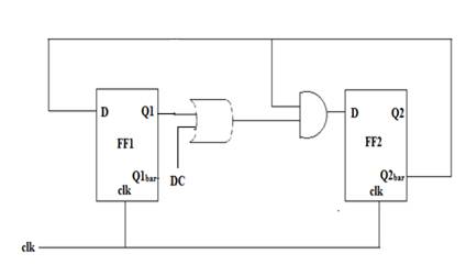
A divide-by-2/3 counter design based on E-TSPC logic proposed by Pellerano [7] is given in Figure 1. This design consists of two E-TSPC based Flip Flops (FFs) and two logic gates i.e., an OR gate and an AND gate. The transistor schematic of the design is depicted in Figure 2. When the divide control signal DC is “0”, the OR gate becomes disabled. The OR gate is merged into the output of FF1 as shown in the transistor schematic to a divide-by-3 function. When the divide control signal DC is “1”, the OR gate has got a steady high output irrespective of the other input[6]. So the output of FF1 will be disabled. Therefore FF2 alone performs the divide-by-2 function. But the major disadvantage with this approach is that there exists redundant power consumption during divide-by-2 operation due to the continuous toggling of FF1 output since the input to the FF1 is not disabled.
Figure 1. Logic Structure of Design I
As a remedy to the above mentioned problem in Design I, another divide-by-2/3 counter design based again on ETSPC logic was proposed in [1] by Xiao Peng Yu as shown in Figure 3. Here the divide control logic is placed at the input of FF1 rather than at the output of FF1 as in Design I. The transistor schematic of the design is also depicted in Figure 4. When DC bar=’0’, output of FF1 becomes frozen i.e.; the output of AND gate is always 0 which makes the input to FF1 always steady. This prevents the following stages from any switching or toggling activities for the purpose of power saving and thus FF2 alone performs divide-by-2 function[8]. But the cone here when compared to Design I is that of the first stage of FF1 itself, and however encounters larger power consumption since the pull up path is turned on all the time and the short circuit current is drawn repetitively whenever the clock signal turns '1'.
This type prescaler design uses two embedded NOR gates instead of an AND gate and an OR gate as the conventional TSPC 2/3 prescaler.

Figure 2: Transistor schematic of Design I
An Extended True-Single-Phase-Clock (E-TSPC) based divide-by-2/3 counter design for low power consumption applications is proposed here. The logic structure of the proposed design is shown in Figure 5. As in previous E-TSPC based designs, Design I and Design II, the proposed design also has two flip flops (FFs) and an AND gate in common. The division control logic is implemented by means of a switch.
As already stated above, the division control logic is implemented here using a switch. When the switch is open, the input from FF1 is disconnected and FF2 alone comes into action and divides the clock frequency by 2. When the switch is close, similar to the Design I and DesignII[1, 7], FF1 and FF2 are linked to form a counter with three distinct states and thus divides the clock frequency by 3. Figure 6 shows the circuit schematic of the proposed design. Other than the two E- TSPC FFs, only one PMOS transistor PDC is needed. The PMOS transistor controlled by the divide control signal serves as the switch[9]. The AND gate plus its input inverter are achieved by way of wired- AND logic using no extra transistors at all. When DC is “1”, the PMOS transistor PDC is turned off as a switch. A single PMOS transistor, however, presents a smaller capacitive load to FF1 than an inverter does in Design I [7]. When DC is “0”, the output of FF1, Q1b, is connected with the output node of the first stage inverter of FF2 (D2b) through the PMOS transistor PDC. In an E-TSPC FF design, the output of the first stage inverter can be regarded complementary to the input, D i.e., Dbar . Therefore, a wired-OR logic is actually implemented.

By applying DeMorgan's law to the above Boolean equation we get,

which is exactly the desired logic as it is quite evident from Figure 8. Since Q1b is applied to the input of D2b (complement of D), the inverter needed to complement the Q1b signal can be eliminated which makes the circuit more simple enhancing the speed and power behaviors. First of all, unlike any previous designs, here the E-TSPC FF design remains intact without any logic embedding thereby the effect of parasitic capacitance is alleviated. Both speed and power behaviors are not affected, which indicates a performance edge over the logic embedded FF design[10]. Secondly, the inverter to complement one of the two E-TSPC FF outputs for divide-by-3 operations is removed in the proposed design in Figure 6. The circuit simplification, again, suggests the improvement in both speed and power performances.
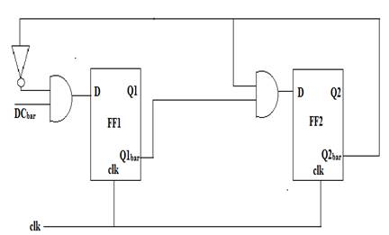
Figure 3. Logic Structure of Design II
Figure 4. Transistor schematic of Design II
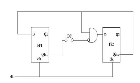
Figure 5. Logic Structure of the Proposed Design
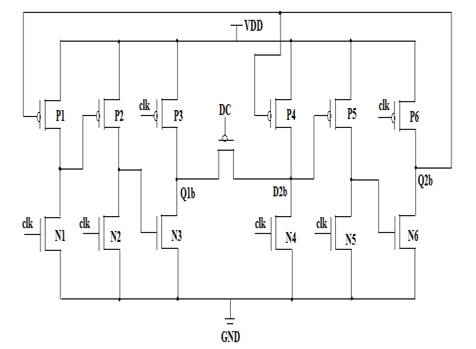
Figure 6. MOS Schematic of the Proposed Design
The proposed wide-band multi-modulus 32/33/47/48 prescaler which can divide the input frequency by 32, 33, 47 and 48 respectively is shown in Figure 7. The multimodulus prescaler is similar to the 32/33 and 47/48 prescaler but with an additional multiplexer to control the switching between 32/33 and 47/48 modes. The proposed prescaler performs additional divisions (divideby- 47 and divide-by-48) without any extra flip-flop, thus saving a considerable amount of power and design complexity.
Besides the usual MOD signal for controlling the division ratios (N/N+1), the additional control signal Sel is used to switch the prescaler between 32/33 and 47/48 modes.
All prescalers were designed using 0.18μm Taiwan Semiconductor Manufacturing Company, Ltd. (TSMC) process technology. The schematic entry was done using Mentor Graphics Design Architect. The post layout Simulation was done using Mentor Graphics ELDO. Delay and energy were averaged over a set of random input vectors and the layout was done using Mentor Graphics IC Station.
All the 2/3 prescaler designs such as Design I, Design II and the proposed prescaler were simulated. Since voltage scaling serves as the principal means for energy reduction, all simulations were conducted with a supply voltage of 0.9V for E-TSPC based circuits and 1.2V for TSPC based circuits as E-TSPC based circuits are sustainable to low VDD operations. The simulation results were analyzed and the total power dissipated was recorded in each case. The Pre layout simulation result of the proposed design is given in Figure 8 (a) and 8 (b).
The power dissipation of all the 2/3 prescalers implemented is shown on Table 1. The comparison results show that the proposed 2/3 prescaler has improved power performance than other designs. The comparison results show that the Power Delay Product (PDP) is less in the proposed design when compared to other implementations. The area was compared after taking layout of all the designs and the layout diagram of the proposed design was obtained. Therefore the proposed design has got 46%, 43% and 39% improved PDP when compared with Design I, Design II and Design III respectively.
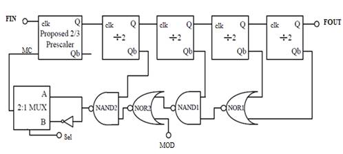
Figure7. Proposed Multi modulus 32/33 & 47/48 Prescaler
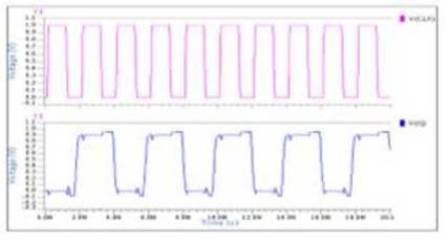
Figure 8. (a): Divide by 2 of Proposed Design
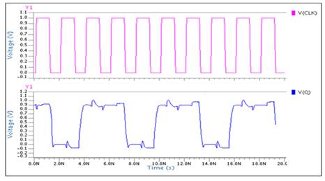
Figure 8. (b): Divide by 3 of Proposed Design
The Pre–Layout simulation of the multimodulus prescaler design were designed. The simulation results were analyzed and the total power dissipated was recorded in each case. On comparison, it proves that the proposed multimodulus prescaler has 20% and 28% better power performance in N and N+ 1 division respectively. Table 2 shows the power comparision of multi modulus 32/33/47/48prescalers.
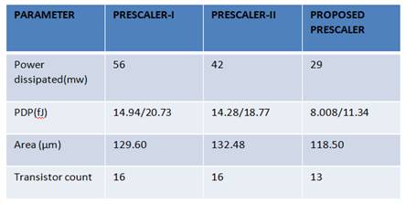
Table1. Comparison of 2/3 Prescalers
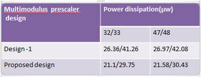
Table 2. Power Comparison of Multimodulus Prescalers
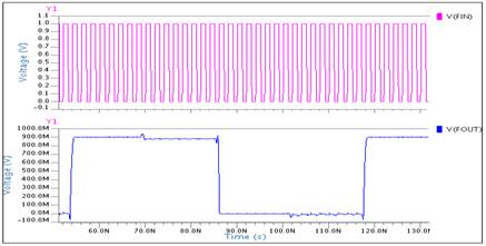
Figure 9. Divide by 32 of 32/33 Prescaler
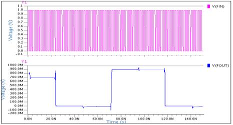
Figure 10. Divide by 47 of 47/48 Prescaler
The Pre–Layout simulation of the 32/33 prescaler design using the proposed prescaler was done as in Figure 9. The total power dissipated obtained are 21.1μW and 29.75μW in division by 32 and 33 modes respectively. The Pre–Layout simulation of the 47/48 prescaler design using the proposed prescaler was done as in Figure 10. The simulation results were analyzed and the total power dissipated was recorded. The total power dissipated obtained are 21.58μW and 30.43μW in division by 47 and 48 modes respectively.
In the proposed design a 2/3 prescaler was implemented using E-TSPC logic. The proposed design is much more area efficient compared to the existing implementations due to the reduced number of transistors required for its implementation. Simulation results show that, compared with the conventional TSPC and E-TSPC based 2/3 prescaler designs as much as 46% in Power Delay Product (PDP), 24% in operation speed and 44% in area can be achieved by the proposed design. Also a 32/33 prescaler, 47/48 prescaler and a multimodulus 32/33/47/48 prescaler which incorporates the proposed 2/3 prescaler were designed and implemented. Simulation results show that the power dissipation of the proposed multimodulus prescaler is lesser than the existing multimodulus prescaler design. The schematic entry was done using Mentor Graphics.