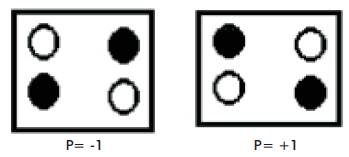
Figure 1. QCA Cell Polarization
Quantum Dot Cellular Automata (QCA) is an emerging nanotechnology in the field of Quantum electronics for low power consumption and high speed of operational phenomenon. Such type of circuit can be used in many digital applications where CMOS [Complementary Metal Oxide Semiconductor] circuits cannot be used due to high leakage and low switching speed. Also, reversible logic is becoming a more and more prominent technology having its applications in low power CMOS, quantum computing, nanotechnology, and optical computing. Reversibility plays an important role when energy efficient computations are considered. By combining both of these low power and area efficient QCA technologies, the author can make a new generation low power system. In this paper, reversible eight-bit parallel binary adder/Subtractor using QCA has been proposed. This method reduces the total area used compared to the normal CMOS based structures and reduces power dissipation by using reversible logic gates.
In the past few decades, the exponential scaling in feature size and the increase in processing power have been successfully achieved by Very Large Scale Integration (VLSI) technology, mostly using CMOS; however, in the not-so-distant future[C. S. Lent, P. D. Tougaw, 1993], [P.Ilanchezhian, R.M.S.Parvathi, 2013] this technology will face serious challenges as the fundamental physical limits of its devices are reached. In the recent years, there has been extensive research at nanoscale to supersede the conventional CMOS using the so-called emerging technologies. It is anticipated that these fundamentally different technologies can achieve extremely high densities and high operational speed. Among these new devices, Quantum-Dot Cellular Automata (QCA) not only gives a solution at nanoscale, but also offers a new method of computation and information transformation (often referred to as processing-in- wire)
Quantum dot cellular automata is used to represent Quantum cells, which are the basic building blocks of Quantum electronics, as CMOS is used in VLSI technology. The basic structures used in the design of QCA digital circuits are the majority gate, inverter and wire. In case of Majority gate 3, 5 and multi-input, majority gates are available. As two logic states [-1 and +1] are established in QCA, it is easy to implement many digital circuits in this technology. The clocking zones which are introduced[A.Gin, S. Williams, H, 1999] serve as platform for designing combinational as well as many sequential circuits. Code converters are often used in digital systems, this paper will provide an easy way to reach the goals effectively. QCA cell is made up of four quantum dots arranged along the corners of a square out of which two are inhabited by electrons.
Producing dots of small positional and size variability usually involves the use of electron beam lithography, which is similar to conventional lithography, except that those patterns are traced out using an electron beam rather than using a mask and light.
A schematic diagram of a four-dot QCA cell is shown in Figure. 1. The cell consists of four quantum dots positioned at the corners of a square. The cell contains two extra mobile electrons, which are allowed to tunnel between neighbouring sites of the cell. The compensating positive charge is fixed and immobile. Tunnelling out of the cell is assumed to be completely suppressed by the potential barriers between cells. It is also possible to add a fifth dot at the centre of the square; the addition of this dot improves the behaviour of the cell slightly, but for simplicity, the authors will focus mainly on the four-dot cell. If the barriers between cells are sufficiently high, the electrons will be well localized on individual dots. The Coulomb repulsion between the electrons will tend to make them occupy antipodal sites in the square as shown in Figure. 1. For an isolated cell, there are two energetically equivalent arrangements of the extra electrons which is denoted as cell polarization P= +1 and P= -1. The term "cell polarization" refers only to this arrangement of charge and does not imply a dipole moment for the cell. The cell polarization is used to encode binary information P= +1which represents binary 1and P= - 1 which represents binary 0.
Figure 1. QCA Cell Polarization
When QCA cells are arranged nearby and one cell is fixed with any one polarization, all the neighbour cells are polarized in the same way because of the columbic interaction. This property of QCA cells lets us to use them as wires. The regular arrangement of these QCA cells forms a binary wire[C. S. Lent, P. D. Tougaw, Feb 1993], through which information can be carried out from one end to other end. Figure. 2. shows the binary wire [C. S. Lent and P. D. Tougaw, Oct 1993], [C. R. Graunke, D. I. Wheeler, 2005]. The left most cell is fixed with a polarization, which is carried out to the right most cell through this arrangement.
Cells which are positioned diagonally from each other tend to anti-align. This feature is employed to construct an inverter as shown in Figure. 3 [P.D. Tougaw and C. S. Lent, Feb 1994]. The anti-alignment can also be seen by examination to be simple on the sequence of the mutual repulsion between electrons and the geometry of the cells. Although two diagonal cells function as an inverter, this more symmetric design ensures exact symmetry between the inversion of a one and a zero.
Figure. 4 shows the fundamental QCA logical device, a three- input majority gate, from which more complex circuits can be built. The central cell, labelled the device cell, has three fixed inputs, labelled A, B, and C. The device cell has its lowest energy state if it assumes the polarization of the majority of the three input cells.
M (A, B, C) = AB+BC+CA
Five inputs majority gate is a new structure used for 3- input AND and OR gate implementation shown in Figure 5. This device can be used to reduce circuit complexity.
Computation in a QCA majority gate is performed by driving the device cell to its lowest energy state, as shown in Figure. 4 and 5. This is achieved when the device cell assumes the polarization of the majority of the three or five input cells. The reason why the device cell always assumes a majority polarization is because it is in this polarization state that the Columbic repulsion between electrons in the input cells is minimized[Himanshu, Thapliyal, 2012]. The polarization of the device cell is then transferred to the output cell.
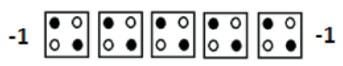
Figure 2. A Binary Wire
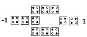
Figure 3. Inverter
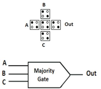
Figure 4. Majority Voting Gate (3-inputs)
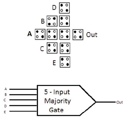
Figure 5. Five input Majority Gate
Fig. 6 shows a pipelined clocking scheme that must be employed for a QCA circuit to function properly. In this scheme, the clock is divided into four phases with each phase incurring a 90 phase delay. The phases are called switch, hold, release, and relaxed[C. S. Lent, P. D. Tougaw, Feb 1993], [Douglas Tougaw, Eric W. Johnson, 2012]. The clocking scheme allows an array of cells to perform a certain computation, have its state frozen by the raising of the inter-dot potential barriers, and have the result of the computation serve as the input to the successor array of cells. During the computation, the successor cell array is kept unpolarized so that it does not influence the computation. Finally, neighboring cell arrays concurrently receive neighboring clock phases.
In the switch phase, the initial state of the QCA cell is unpolarized and the inter-dot potential barriers are kept low. The barriers are then raised and the cells become polarized according to the state of their neighboring (input) cells. It is in this state where the actual computation is performed. In the hold phase, the cell states are fixed and the potential barriers are held high so that the cells can serve as inputs to the next stage. In the release phase, the potential barriers are lowered and the cells are allowed to relax to the unpolarized state. Finally, in the relaxed state, the potential barriers remain low and the cells remain unpolarized.
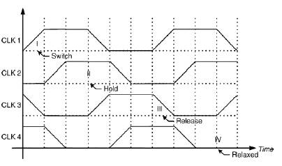
Figure 6. Four phase clocking scheme of QCA
Reversible computing was started when the basis of thermodynamics of information processing showed that conventional irreversible circuits unavoidably generate heat because of losses of information during the computation. The different physical phenomena can be exploited to construct reversible circuits avoiding the energy losses. One of the most attractive architecture requirements is to build energy lossless small and fast quantum computers. Most of the gates used in digital design are not reversible, for example NAND, OR and EXOR gates.
A Reversible circuit/gate can generate unique output vector from each input vector, and vice versa, i.e., there is a one to one correspondence between the input and output vectors. Thus, the number of outputs in a reversible gate or circuit has the same as the number of inputs, and commonly used traditional NOT gate is the only reversible gate. Each Reversible gate has a cost associated with it called Quantum cost. The Quantum cost of a Reversible gate is the number of 2*2 Reversible gates or Quantum logic gates required in designing. One of the most important features of a Reversible gate is its garbage output i.e., every input of the gate which is not used as input to other gate or as a primary output called garbage output.
In digital design, energy loss is considered as an important performance parameter. Part of the energy dissipation is related to non-ideality of switches and materials. Higher levels of integration and new fabrication processes have dramatically reduced the heat loss over the last decades. The power dissipation in a circuit can be reduced by the use of Reversible logic. Landauer's [C. S. Lent, P. D. Tougaw, Feb 1993], [K. Hennessy and C. S. Lent, Sep 2001] principle states that, irreversible computations generate heat of K*Tln2 for every bit of information lost, where K is Boltzmann's constant and T, the absolute temperature at which the computation is performed. Bennett[C. S. Lent, M. Liu, 2006] showed that, if a computation is carried out in Reversible logic, zero energy dissipation is possible, as the amount of energy dissipated in a system is directly related to the number of bits erased during computation. The design that does not result in information loss is irreversible. A set of reversible gates are needed to design reversible circuits. Several such gates are proposed over the past decades.
Arithmetic circuits such as Adders, Subtractors, Multipliers and Dividers are the essential blocks of a Computing system. Dedicated Adder/Subtractor circuits are required in a number of Digital Signal Processing applications. Several designs for binary Adders and Subtractors are investigated based on Reversible logic. Minimization of the number of Reversible gates, Quantum cost and garbage inputs/outputs are the focus of research in Reversible logic.
The main object in reversible logic theory is the reversible function, which is defined as follows.
Definition1.
The multiple output Boolean function
F(x1; x2; :::; xn) of n Boolean variables is called reversible if:
1. The number of outputs is equal to the number of inputs;
2. Any output pattern has a unique preimage. In other words, reversible functions are those that perform permutations of the set of input vectors.
Definition2.
Garbage is the number of outputs added to make an ninput k-output function ((n; k) function) reversible. The authors use the words "constant inputs" to denote the present value inputs that were added to an (n; k) function to make it reversible. The following simple formula shows the relation between the number of garbage outputs and constant inputs. Input + constant input = output + garbage. The Quantum Cost of 1*1 Reversible gates is zero, and Quantum Cost of 2*2 Reversible gates is one. Any Reversible gate is realized by using 1*1 NOT gates and 2*2 Reversible gates, such as V, V+ and FG gate which is also known as CNOT gate. The V and V+ Quantum gates have the property given in Equations 1, 2 and 3.

The Quantum Cost of a Reversible gate is calculated by counting the number of V, V+ and CNOT gates [H Thapliyal and N Ranganathan, 2009],[ C. S. Lent, P. D. Tougaw, 1993].
The simplest Reversible gate is NOT gate and is a 1*1 gate. The Reversible 1*1 gate is NOT Gate with zero Quantum Cost is as shown in Figure 7.
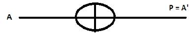
Figure 7. NOT gate
Controlled NOT (CNOT) gate is an example for a 2*2 gate. The Reversible 2*2 gate with Quantum Cost of one having mapping input (A, B) to output (P = A, Q = A B) is as shown in Figure 8.
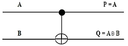
Figure 8. Feynman/CNOT gate
The 3*3 Reversible gate with three inputs and three outputs. The inputs (A, B, C) mapped to the outputs (P=A, Q=B, R=A.B C) is as shown in Figure 9.
Toffoli gate[C. S. Lent, P. D. Tougaw, Feb 1993] is one of the most popular Reversible gates and has Quantum Cost of 5
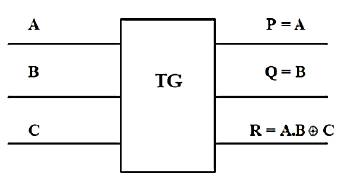
Figure 9. Toffoli gate
The three inputs and three outputs i.e., 3*3 reversible gate having inputs (A, B, C) mapping to outputs (P = A, Q = A B, R = (A.B) C). Since it requires 2 V+, 1 V and 1 CNOT gate, it has the Quantum cost of 4. (Figure 10).
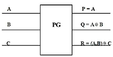
Figure 10. Peres gate
Reversible 3*3 gate maps inputs (A, B, C) to outputs (P=A, Q=A'B+AC, R=AB+A'C) having Quantum cost of 5 and it requires two dotted rectangles, which is equivalent to a 2*2 Feynman gate with Quantum cost of each dotted rectangle is 1, 1 V and 2 CNOT gates. Fredkin gate is shown in Figure 11[C. S. Lent, P. D. Tougaw, Feb 1993].
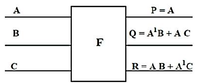
Figure 11. Fredkin gate
Reversible half Adder/Subtractor design is implemented using two reversible gates as shown in Figure 12, of which two are FG gates each having Quantum cost of one and a PG gate, with Quantum cost four. The number of Garbage outputs is two i.e., g1 and g2, Garbage inputs are the one denoted by logical zero and Quantum Cost is six.
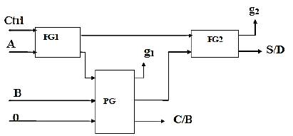
Figure 12. Reversible Half adder/subtractor
The Reversible Full Adder/Subtractor Design using reversible gates consists of two FG, two PG gates, and their interconnections are shown in Figure 13. The three inputs are A, B, and Cin. The outputs are S/D and C/B. For Ctrl value zero the circuit performs addition, and Subtraction for Ctrl value one. The numbers of Garbage inputs are 1 represented by logical zero. The Garbage outputs are 3 represented by g1 to g3. The Quantum Cost for the design is 10.

Figure 13. Reversible Full adder/subtractor
Implementation of reversible adder-cum-subtractors using QCA for the structures shown in Figure 12 and 13 is done with the help of QCA Feynman gate and Peres gate.
This Feynman gate architecture consists of 119 cells and 2 occupies a total area of 0.20µm2 .
This Peres gate architecture consists of 193 cells and 2 occupies a total area of 0.34µm2 .
By combining these two architectures, the author can design many digital circuits of high speed, low power and reduced area.
Compared to the CMOS architecture designs which are in trend now, these reversible Feyman gate shows better results as shown in Figure 16. Here, the authors are getting the result in second clock cycle. It means that, it is taking one clock cycle to change the initial steady state polarization.
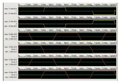
Figure 16. Simulation result for the input combination A=1, B=1
Simular to Feyman gate, Peres gate produces its output in the second clock cycle as shown in Figure 17.
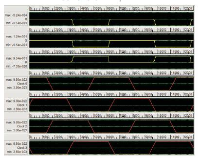
Figure 17. Simulation result for the input combination A=1, B=1, C=1
The Half and Full Adder/Subtractor Figures 12 and 13 and their QCA implementations in Figures 14 and 15 are used to construct Reversible eight-bit Parallel Binar y Adder/Subtractor which is shown in Figure 18. The ctrl input is used to differentiate eight-bit addition and subtraction functions. The two eight-bit binary numbers are A0 to A7 and B0 to B7. Carr y/Borrow is obtained after Addition/Subtraction and is represented by C_B1 to C_B7. The outputs Sum/Difference and Carry are shown as S_D0 to S_D7 and C_B8, respectively. The implementation requires seven Full Adder/Subtractor units and one half Adder/Subtractor units in which first stage is half Adder/Subtractor.
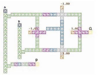
Figure 14. Feynman gate
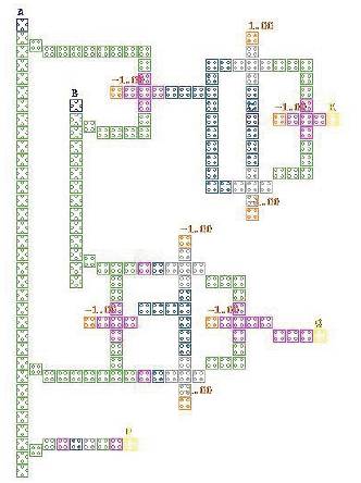
Figure 15. Peres gate
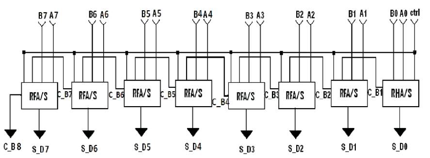
Figure 18. Reversible Eight-bit parallel Binary Full Adder/Subtractor
The existing Reversible Binary Subtractor based on Reversible gates[H Thapliyal and N Ranganathan, 2009] to implement full Subtraction requires a Quantum Cost of 12, Garbage inputs of one and Garbage outputs of two. The proposed Reversible eight-bit Parallel Binary Adder/Subtractor Design showed in this paper is better compared to the existing design in terms of Quantum Cost, Garbage inputs and Garbage outputs and also in our design, the Full Subtraction and Addition function is implemented together as compared to only Subtractor in the existing design. Also QCA implementation is the specific part which increases the switching speed and reduces area. So the conclusion is that, totally this combination of reversible logic and QCA gives the best results which cannot be expected using any other methodologies.