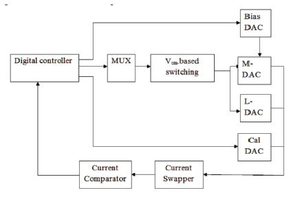
Figure 1. Functional block diagram of proposed self-calibrated 12-bit DAC.
This paper focuses on Foreground Calibration technique. For high speed and high resolution video applications, current steering DAC is preferred. In large current sources, linearity error is introduced and detected by using two current tunning loops and digital controller. In this paper, Vcm based switching method is injected between MUX (Multiplexer) and DAC to compensate the error which reduces the time of operation. For 12-bit DAC prototype realized 90nm CMOS process,90% gate area reduction current source array is achieved. The measurement result demonstrates that the calibrated converter achieves both DNL (Differential Non-Linearty) and INL (Integral Non-Linearity) less than 1LSB.
In high speed electronics, a digital-to-analog converter (DAC) is used to convert digital data into an analog signal. There are several DAC architectures used for a particular application. Each DAC is determined by the following six main parameters: physical size, power consumption, resolution, speed, accuracy, cost. The audio DAC is a low speed high resolution technique while the video DAC is a high speed low to medium resolution type. Most the very high resolution DACs are of this type due to its high linearity and low cost without large current sources using techniques such as self-calibration [1], and INL shaping [2]. Thus a new foreground calibration technique is used for applications of high speed, high linearity and low voltage which compensates for the current source mismatches shrinking the die size and hence reduceing area [3]. Background schemes can perform continuously while ADC is needed. Background calibration technique is used to avoid mismatch errors. It does not split the sampling capacitor to avoid calibration time and calibration speed four times faster when compared to other techniques [4]. The DAC architecture of multiple parallel sub-DAC is used. In this architecture the unused sub-DAC can be switched off in order to reduce power consumption [6]. Sigma-delta technique is used for high resolution at low cost [5]. The novel architecture features multiple parallel sub-DAC unit cores. The parallel sub-DAC units can be used together or separately to achieve mixed signal application. The various matching parameters such as threshold voltage and current factor of several process are compared. DAC with resolution from 8 to 16 bits are split into two or more segments. Each segments have number of bits. Finally the sufficient INL and DNL accuracy for the overall resolution of DAC is obtained [7]. The matching properties of the threshold voltage, substrate factor, and current factor of MOS transistors have been analyzed and measured [8]. These matching properties are taken into account by the use of time consuming and CPU intensive Monte Carlo simulations [9]. The various calibration schemes are not suitable for very low voltage applications but new Foreground Calibration techniques are only suitable. Normally, capacitor mismatches as well as gain error are caused by unbalanced array capacitance [10]-[12]. In this paper, Vcm based switching methods are injected between the DAC to reduce mismatches and increase the speed. For 12-bit DAC prototype realized 90nm CMOS process,90% gate area reduction current source array is achieved. The measurement result demonstrates that the calibrated converter achieves both DNL and INL less than 1LSB.For high frequency, low SNDR value and for low frequency, high SNDR should be obtained. Various types of DAC are used for specified applications but in this paper only current-steering DAC is used for low resolution which achieves high speed at low cost. Finally, Monte Carlo simulation shows that number of samples are deviated and various specifications are obtained.
The proposed calibration scheme is applied to a 12-bit, 400-Msamples/s DAC prototype, which is illustrated in Figure. 1. To guarantee monotonicity and reduce glitch power, the main current cell array is divided into a 4-bit MSB array (M-DAC) and an 8-bit LSB array (L-DAC). The lower 4 bits consist of binary-weighted current cells. The middle 4 bits and upper 4 MSBs are with unary current cells. The calibration hardware includes a calibration DAC (CalDAC), a BiasDAC, a current comparator, a digital controller, data registers, and other control circuits.
The current comparator compares two analog signals and produces one digital signal. The digital controller receives video synchronization pulses (Hsync and Vsync) and manipulates calibration phases and test patterns. The MUX selects the 12-bit input from the digital controller or the external input DIN[11:0]. The current swapper used before the current comparator re-routes each input signal to any of the two outputs, depending on a control signal swap. The exact mechanism for assigning tolerance values varies by country and industry type. The measuring equipment manufacturer generally assigns the measurement tolerance, suggests a calibration interval and specifies the environmental range.
Figure 1. Functional block diagram of proposed self-calibrated 12-bit DAC.
A very common interval in the United States for 8–12 hours of use of 5 days per week is six months. The same instrument in 24/7 usage would generally get a shorter interval. The assignment of calibration intervals can be a formal process based on the results of previous calibrations. Larger area current sources is therefore inevitable for a high-resolution DAC. Nonetheless, if we can adopt small dimension current sources but still meet the accuracy criteria, overall die size can be shrinked with lower production cost
The calibration procedure mainly focuses on the unary MDAC. In the current source cell adopted pMOS 2.5-V thickoxide device with minimum length to accommodate large swing for video applications. The L-DAC is composed of binary-weighted current sources, which are realized by connecting 255+1 unit conversion cells in parallel. The L-DAC remains uncalibrated; its gate area is not as large as the area used for a 12-bit intrinsic DAC.
The offset current can be eliminated by adjusting the current mirrored to the M-DAC with the help of digital controller. In order to reduce area, feature size of unit MDAC current source is only 16 times of unit area used in the L-DAC.
Figure.2 shows that each unary current source in the MDAC is composed of 256 unit current sources, its expected current is equal to the overall output current of the LDAC, i.e.,255+1. The expected current with the shrinked current source is deviated with an offset current Ie.Compared with the conventional current detection approach; this method doubles the detection range by utilizing both differential outputs of the CalDAC.
In the calibration, two steps must be followed which are “offset tuning” and “mismatch tuning”. During the calibration period, the digital controller allocates the current flow of the current source array.
When using the supply as reference, the switching power is dynamic, which is correlated with the switching sequence. During the global sampling phase, the input signal Vin is stored in the entire capacitor array. The conversion begins only by switching the MSB capacitor to VDD and others to GND. The Vcm based switching method halves the array capacitance leading to around 90% energy saving when compared with the conventional one.
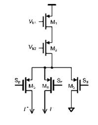
Figure 2. current cell structure
Figure.3 shows that Vcm -based switching algorithm. In the sampling phase φ1,Vin stored in the capacitor and Vout of the capacitor array. If –Vin < 0,Sm-1 goes to GND and -Vin > 0, Sm,k-1 is switched to VDD. If MSB capacitor is not required anymore, so that it can be removed from n-bit DAC array, next (n-1) bit array is switched, instead of n-bit. It can be reduced to half capacitance reduction compared to other method.
The Vcm based approach performs the MSB transition by connecting the differential arrays to Vcm . This switching charges 75% less capacitance. When compared with conventional switching, it can reduce reference buffer.
The power dissipation is derived from the bottom of the parasitic capacitive arrays, while in the conventional charge-redistribution where the necessary MSB “up” transition costs significant switching energy and settling time. The MSB capacitor is not required anymore, it can be removed from the n-bit DAC array. The next n −1 estimation is done with an (n −1) bit array instead of n-bit counterpart, leading to half capacitance reduction with respect to the conventional method.
The Vcm -based method achieves half capacitance reduction when compared with the conventional one. Thus, this method is used to reduce the DNL by half when compared with the conventional method. It prevents the occurrence of large switching transient. In every bit cycle, only one capacitor is switched without wasting energy and settling time.
While the offset current is eliminated, mismatches among the MSB current cells still limit the overall linearity. Figure.4 illustrates the current errors for different MSB inputs after offset tuning are ∑ki=1δi where i is the decimal equivalent value of DIN[11:8]. It is mentioned that, ideally, this error increased MSB input does not continuously accumulate, since the average of δi is approximately zero. In reality, the average of di is limited by the finite resolution of offset tuning. This residual error should be covered during the mismatch tuning. An 8-bit CalDAC with a step size of 0.1Iμ and maximum error are reduced and so shrinked the device size.
Due to the large mismatches between them the current sources are limited by the calibration technique to ensure that power saving and area are achieved. The current comparator will compare two inputs IP and IN, and feedback a new value to adjust the current distribution between and ICal,P. and Ical,n will approach each other.
General display monitors receive five types of data signals: Red, Green, Blue, Horizontal Sync (Hsync), and Vertical Sync (Vsync). The last two signals, either in analog or digital display systems, provide timing information to correctly display the pixel data. In reality, there are periodic time intervals, called Hsync blanking and Vsync blanking which do not have visible data information in them. In general applications for a HDTV (High Definition Television) format operating at 1080p with 60 Hz refresh rate, the Hsync blanking and Vsync blanking are 1.88 and 667 μs, respectively. Calibration routines can be inserted into these time intervals without interrupting the normal operation.
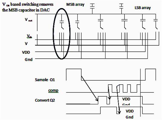
Figure 3. Vcm based switching
The current sources in L-DAC and calDAC are placed with common centroid style to 8-bit intrinsic matching. The MSB current sources are placed side by side without any complicated routing in order to to compensate the mismatches when Vcm-based switching added between the MUX and DAC. Using the switching is method half capacitance reduction can be achieved. This DAC was fabricated in a standard 90-nm CMOS process. The active area is 0.18 mm2 per channel. The digital controller occupies less than 5% of the total area.
Most errors in the INL and DNL profiles before calibration and static linearity also results in poor dynamic performance Nonlinearities are chiefly from the finite resolution of the CalDAC and the intrinsic matching of the non calibrated L-DAC. The calibration optimization used in this structure have provided a dramatic reduction and die area when compared to the same performance level without calibration. Before calibration the maximum INL, DNL and SNDR range increase when compared toconventional one. But, after calibration, the maximal INL and DNL is less than 1LSB. SNDR degrades depending on different input frequencies. During the foreground calibration technique the mismatches are compensated and area is also reduced. To ensure this technique area, power and mismatches are also reduced and stable power, ground analog digital blocks use separate power lines.
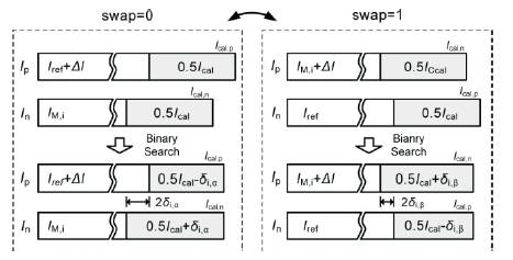
Figure 4. Calibration procedures of mismatch tuning
The large switching transient leads to insufficient DAC settling and supply ripples. The effect of parasitic capacitors of split DAC is not a dominant factor. So the calibration technique is applied to correct all the large nonlinearity codes. Figure.5 illustrates the simulation results of calibrated DAC, which describes the results of 400 samples of Monte Carlo simulation runs that are best straight line plotted. Figure.6 Shows the simulation of INL and DNL which perform the operation and provides the analysis descriptions. Figure.7 illustrates the various values of tolerance and parameter changed and shows the simulation results. Finally the expected simulation results of the performance and comparisons of other calibrated DACs. are shown in Table 1. With shrinked current sources and error compensation schemes of relatively small dimension, the proposed calibration saves the DAC cost and low frequency variation recalibrated during the blanking pulses.
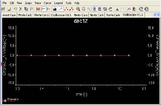
Figure 5. Simulation results of calibrated DAC
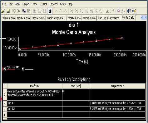
Figure 6. Behavioral simulation results of DNL and INL
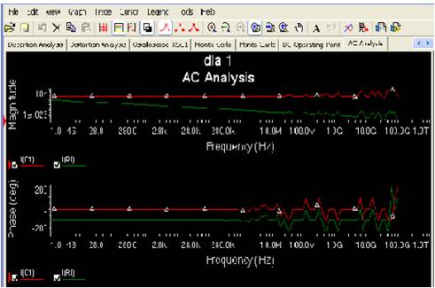
Figure 7. Simulation Results of Calibrated DAC with AC Analysis
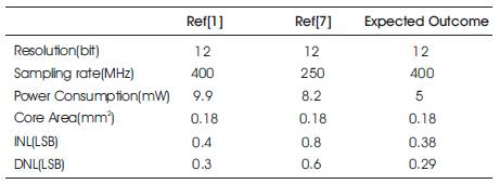
Table 1. Comparision of Other Calibrated DACs
For self-calibrated 12-bit DAC operating tens of MS/s with Vcm-based switching are used. In this paper Foreground Calibration scheme for high resolution current-steering DACs is used in video display systems. The Vcm-based switching technique provides conversion linearity when compared with the other methods in every bit cycle. Only one array capacitor is switched without wasting energy. Digitally-assisted solution based on measuring and compensating current mismatches with two tunning loops improves static performance with small silicon area due to only 4-bit accuracy of the M-DAC and 8-bit accuracy of the L-DAC. Measurement results demonstrate that both high speed and low power is achieved by using Vcm-based switching, when it decides to send digits to the calibration. Monte Carlo Analysis shows how much percentage of circuit meet specifications. It calculates the response of the circuit to change the tolerance value, and also reduce mismatches.