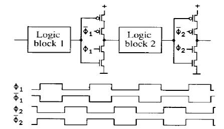
Figure 1. Four phase clock
In this paper, the leakage power and speed performances of extended-true single phase clock and MTCMOS using true single phase clock prescaler are investigated. Based upon this study, MTCMOS technique is implemented in True Single Phase Clock logic DFF design. By using a wired OR logic, only one transistor is used for both mode selection and counting logic systems. The working frequency of the counter is enhanced and the critical path is reduced between the DFF. Using MTCMOS technique static leakage power is reduced and the speed performances are improved. The designed counter is compared in terms of power consumption using DSCH (Digital Schematic Editor & Simulator) and Micro wind tools.
High speed and low power are two major roles and challenges in modern communication systems. Both the above terms are directly proportional to the clock pulses of the system. In olden days, four phase clock techniques as shown in Figure 1 were used, therefore speed of the operation was decreased and the skew problems also arose. To overcome that problem, a two-phase clock signal is used which increases the speed of operation using CMOS technique [1]. Furthermore, TSPC logic is used to increase speed and reduce the delay in CMOS technique. A TSPC design adopts a simpler structure and improves the speed performances [2]. Therefore, a TSPC technique is used and it designs the delay flip flop. Using this flip flop, counter and frequency synthesizer circuit is designed.
Figure 1. Four phase clock
To reduce the number of transistors and area of the circuit, an E-TSPC technique is used to design the DFF. This technique can operate at dual module and it follows some composition rules[3] to design the circuit for low power consumption and circuit simplicity. An operating frequency of E-TSPC is high compared with TSPC.
In E-TSPC, short circuit power dissipation is high compared with TSPC system. During transition the direct short between the supply and ground is high in Extended True to the Single Phase Clock system as shown in Figure 2.
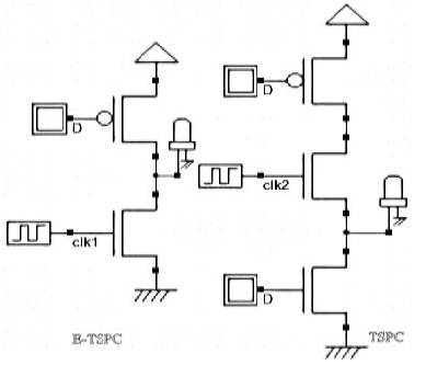
Figure 2. Schematic of the first stage of E-TSPC and TSPC
In this paper, a Multi Threshold voltage based CMOS technique is implemented in TSPC logic design. This enhances the speed and reduces the leakage power in circuits. MTCMOS and voltage scaling are two of the low power techniques used to reduce the power consumption. When technology scales down, total power dissipation will decrease and at the same time delay varies depending upon the supply voltage, threshold voltage aspect ratio , oxide thickness, load capacitances [4][5]. A CMOS device scales downward aggressively in each technology generation to achieve high integration density. In this paper, MTCMOS technique DFF is used to design the counter and to analyse the result between E-TSPC and MTCMOS technique [6].
In this section, the power consumption and operating frequency of the TSPC and E-TSPC based flip flop are analyzed. At each stage, an E-TSPC flip flop uses only two transistor ,but TSPC flip flop requires three transistor [7] as shown in Figure 3.
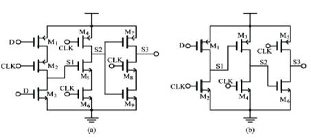
Figure 3. (a) TSPC flip flop (b) E-TSPC flip flop.
In various dynamic logic CMOS circuit techniques, TSPC dynamic CMOS circuit needs only one clock signal for operating the circuit, therefore clock skew problems are avoided. But the load capacitances of E-TSPC flip flop is lower than that of TSC flip flop ,but a switching power for the TSPC flip flop is high since it is directly depends on the output load capacitances as
Pswitching=fclkCLVdd2Where CL is the load capacitances and fclk is the operating frequency. A short circuit power is a period during which a direct path exists between the supply voltage and ground. The short circuit power depends upon the size of transistor and rise and fall time of the input signal. The lesser load capacitances results in lower short circuit power , but the E-TSPC flip flop uses less switching power and it significantly consumes more short circuit power [8]. For each fixed DC level (0.7V-1.2V) the amplitude of the clock signal is varied from 400-600mv and its input signal D is varied from logic'0' to logic'1' with rise time of 70Ps.
In both cases E-TSPC stage consumes more power compared with TSPC stage. In every design, the main aim is to reduce the power consumption and increase the operating frequency. The simulation result indicates that the E-TSPC circuit DC level variation in power consumption is high as shown in Figure 4. In TSPC the DC level variation is small compared with E-TSPC, but the power consumption remains constant. E-TSPC circuits need large amplitude level compared with TSPC. Therefore, the analysis suggests that TSPC is better choice for low power application [9]. In this paper, a MTCMOS technique is implemented in TSPC logic system to design the DFF for counter design.
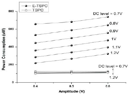
Figure 4. Power consumption against different DC levels and amplitude of clock signal for single stages of E-TSPC and TSPC..
Multithreshold voltage based CMOS is one of the most important technique for power reduction which effectively reduce the leakage power. It operates in two modes such as (a) high threshold mode and (b) low threshold mode. In high threshold mode the leakage power dissipation is reduced and low threshold mode is used to improve the speed of circuits. To achieve the above properties, sleep and sleep bar transistor are required. A PMOS transistor is used for sleep bar transistor and NMOS transistor is used for sleep transistor as shown in Figure 5. A negative pulse is used to activate the NMOS transistor and positive pulse is used to active PMOS transistor.
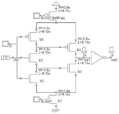
Figure 5. MTCMOS D Flip Flop.
A supply voltage is directly connected to the drain of sleep bar transistor and ground terminal is directly connected to the source terminal of the sleep transistor. Both sleep and sleep bar gate terminals are connected to the clock pulse for activation. If a clock pulse is high, a sleep transistor is active and sleep bar transistor is de-active, therefore a circuit may act as a normal mode (high threshold mode). In normal mode, a circuit has no power supply and it goes to OFF state to reduce the static leakage power. While in OFF state, a transistor can be active by increasing the threshold voltage of transistors (i.e high threshold voltage). For low clock pulse, a sleep bar transistor is active and sleep transistor is de-active and a circuit acts as low threshold mode.
To reduce leakage power in MTCMOS circuits, sleep and sleep bar transistors are operated with high threshold voltages. When sleep input is OFF and sleep bar input is ON, there is no current flow in the low threshold voltage main circuit. When sleep is ON and sleep bar is OFF, then the circuit works in normal Mode. The above circuit is a NMOS based TSPC circuit; a clock signal is given to the input of the NMOS gate terminal. An NMOS based TSPC circuit consumes low power and high speed when compared to PMOS based TSPC circuits. From Figure 5, M6 is the sleep bar transistor and M7 is the sleep transistor. An input signal is given to gate terminal of M1 and M3. A clock signal is given to the input of M2 gate terminal. A brief explanation of operation is shown in Table1.
Two DFF, AND gate and pass transistor are used to design divide 2/3 counter [10]. Depending upon the pass transistor switch a circuit may act as either divide by 2 or divide by 3 operations in circuit. When DC=1 only the second flip flop (DFF2) is active, therefore a circuit should act as divide by 2 operation. When DC=0 an output of DFF1 is given to input of DFF2 with AND operation of DFF2 ouput and it act as divide by 3 operation.
In previous design an E-TSPC technique is implemented to design a DFF as shown in Figure 6 using TSPC techniques, but in this paper MTCMOS technique is implemented to design the DFF using the TSPC logic system. Only the design structure is varied from previous design and its functional operation is similar to each other. A PMOS transistor is used to control the divide operation and it acts as a switch. DFF contains only one input data for operation and its circuit design is very simple and easy to design for application. Depending upon the clock signal, it may act as a switch and it consumes low power. In positive edge DFF, an output may change depending upon the positive edge pulse and inverse in negative edge DFF.
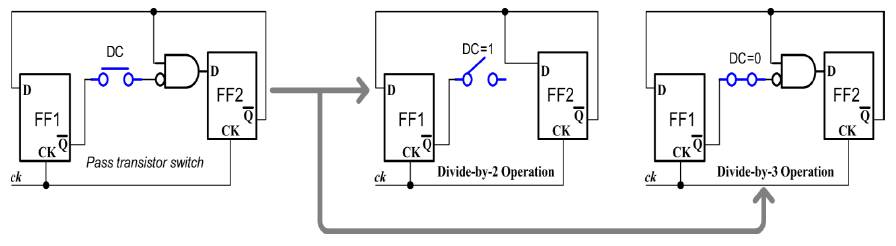
Figure 6. Logic Structure of Divide by 2/3 Counter
Figure 7. is E-TSPC based divide by 2/3 counter with pass tansistor logic technique. Similar operation can be done using MTCMOS technique using TSPC logic structure. A sleep and sleep bar transistor can be implemented in TSPC circuit to perform MTCMOS logic operation in DFF as shown in Figure 8.
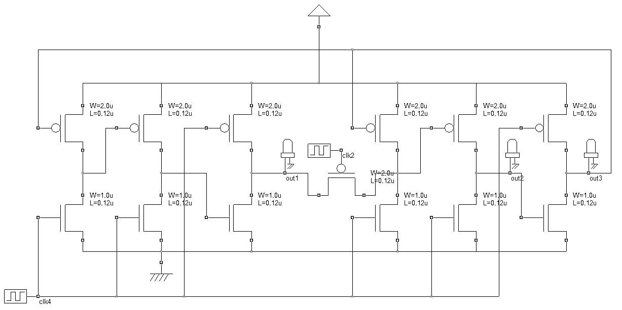
Figure 7. MOS schematic E-TSPC based divide by 2/3 counter with pass transistor logic technique.
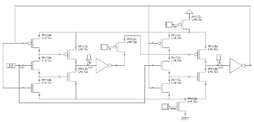
Figure 8. MTCMOS schematic TSPC based divide by 2/3 counter with pass transistor logic technique.
In E-TSPC, the short circuit power dissipation is high compared with TSPC. Large load capacitances in any circuit may leads, to high power dissipation. In TSPC technique, load capacitances are high compared with ETSPC. In MTCMOS system, clock signal is applied to only single NMOS transistor, but in E-TSPC systems a clock is applied for three transistors. Therefore, the clock skew problem is avoided and the power dissipation is reduced in MTCMOS system.
Figure 9. shows the simulation result of existing E-TSPC DFF implemented in Mentor Graphics EDA tool. D flip flop was implemented using extended True Single Phase Clock and power consumption is more since it takes much power during transition.
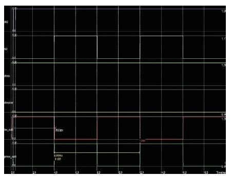
Figure 9. Simulation result for E-TSPC based DFF
Figure 10. shows the Simulation result for MTCMOS based DFF done with Modelsim. The D flip flop was implemented by using Multi Threshold Complementary Metal Oxide Semiconductor.
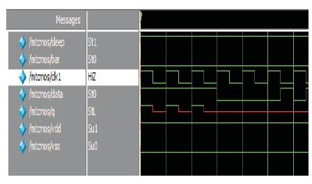
Figure 10. Simulation Result for MTCMOS Based DFF
Compared with E-TSPC based counter, transistor count is high in MTCMOS based TSPC system. Using this DFF, a divide 2/3 counter can be designed and the given frequency can be divided. An E-TSPC based DFF consumes more power compared with MTCMOS technique DFF. An MTCMOS system required two types of threshold circuits like high threshold and low threshold level, therefore it gives complexity to the circuits.
Figure 11. shows the simulation result of divide by 2 counter implemented in Mentor Graphics EDA Tool. D flip flop was designed by using Extended True Single Phase Clock and total power consumption is more in the existing method.
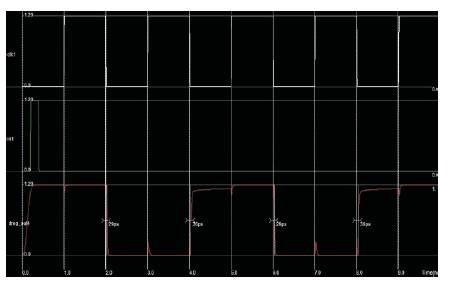
Figure 11. Simulation Result for divide by 2 counter
Figure 12 shows the simulation result of divide by 3 counter implemented in Mentor Graphics EDA Tool. D flip flop was designed by using Extended True Single Phase Clock and total power consumption is more in the existing method. From Table 2, the power consumption between E-TSPC based DFF and MTCMOS based DFF can be calculated. The static leakage power is reduced in MTCMOS based systems. Micro Wind, DCSH Tools, Modelsim and Mentor Graphics EDA Tools are used to calculate the power between the DFFs.
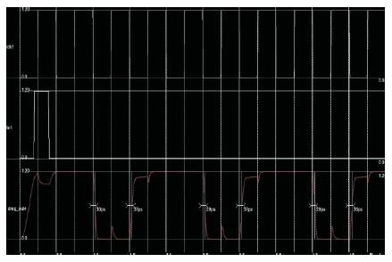
Figure 12. Simulation Result for divide by 3 counter
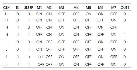
Table 1. MTCMOS Based DFF Operation
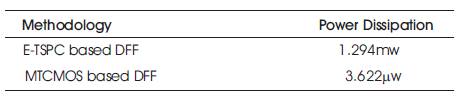
Table 2. Power Consumption Comparison
This paper has presented a MTCMOS based D Flip Flop for the design of divide by 2/3 counter. Even though the number of transistor is high in MTCMOS based DFF system, it consumes low power. In MTCMOS system, clock signal is applied to only single NMOS transistor, but in E-TSPC systems a clock is applied for three transistors. Therefore the clock skew problem is avoided and the power dissipation is reduced in MTCMOS system.