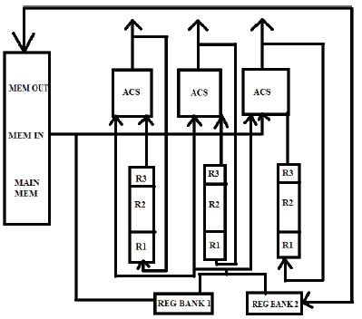
Figure 1. Energy Efficient LUT-Log BCJR Architecture
Wireless Sensor Network can be considered to be energy constrained wireless scenarios, since the sensors are operated for extended periods of time, while relying on batteries that are small, lightweight and inexpensive. Energy constrained wireless application is done with the help of Lookup Table-log-BCJR (LUT-Log-BCJR) architecture. In our existing system the conventional LUT-Log-BCJR architecture have wasteful designs requiring high chip areas and hence high energy consumption for Energy constrained applications. This motivated our proposed System the LUT log BCJR which is designed with Clock gating technique and achieves low-complexity energy-efficient architecture, and a low area and hence a low energy consumption, and also achieving a low energy consumption has a higher priority than having a high throughput. we use most fundamental Add Compare Select (ACS) operations and it is having low processing steps, so that low transmission energy consumption is required and also reduces the overall energy consumption.
Third generation (3G) mobile communication systems aim to provide a variety of different services including multimedia communication. This requires digital data transmission with low bit error rates. However, due to the limitation of the battery life of wireless devices, transmitted power should remain as low as possible. Parallel concatenated encoders consist of two or more component encoders for convolution codes. Decoding is performed iteratively. The output of the first decoder is permutated and fed to the second decoder to form one cycle of the iteration. This reduction in is offset by the turbo decoder's energy consumption, as well as the (typically negligible) energy consumption of the turbo encoder. Low transmission duty cycles and low average throughput less than 1Mbit/seconds [1], [2].
Transmission energy Ebtx (measured in J/bit) dominated the sensor energy consumption because they are separated by up to 1km.Turbo codes are designed to minimize the overall energy consumption [Ebtx+Ebpr] [3] Ebtx means transmission energy and Ebpr refers to the turbo decoder's energy consumption. This reduction in transmission energy is offset by the turbo decoder's energy consumption as well as energy consumption of turbo encoder. [4] Near-capacity coding gain of turbo codes facilitates reliable communication when using reduced transmission energy Ebtx. In the 3rdGeneration Partnership project 3GPP Long Term Evolution (LTE),of turbo codes facilitates transmission throughputs excess of 50Mbits/s in cellular standards. Throughputs that are excess of 100Mbit/s[5][ 6] designed for ASIC(Application- Specific Integrated Circuits) turbo decoder architecture by using MAX-Log BCJR turbo decoding algorithm [7],MAX-Log BCJR algorithm used for low turbo decoder complexity. Overall energy consumption of Ebtx + Ebpr of sensor nodes separated by dozens of meters is the disadvantage of MAX-LOG algorithm. The optimal Log BCJR algorithm is compared with the MAX-Log BCJR algorithm [8] which achieves coding gain by 0.5db.
Due to some demerits obtained in the MAX-LOG algorithm, LUT- Log-BCJR algorithm designed for energy constrained scenarios and the throughput obtained is high when compared to the previous one [9].Low complexity turbo decoder architecture setup has been designed with the ACS unit [10] which facilitates a reduction of overall energy consumption by 10%.To increase the high throughput and low energy, decomposing the ACS unit with the clock gating is done based on the BCJR algorithm.
LUT-Log BCJR architecture is used for energy-constrained scenarios, which avoids the wastage of energy that is inherent in the conventional architecture. It produces an architecture comprising of only a low number of inherently low complexity functional units, which are collectively capable of performing the entire LUT-Log-BCJR algorithm. Further wastage is avoided, since the critical paths of our functional units are naturally short and equallylengthened, eliminating the requirement for additional hardware to manage them. The functional unit that is capable of performing ACS operations, while maintaining a short critical path and a low complexity.
Some of the previous works of the LUT-Log-BCJR algorithm comprised only additions, subtractions and the max* calculations. While each addition and subtraction constitutes a single ACS operation, each max* calculation can be considered equivalent to four ACS operations. In the general case, where Z >0 fraction bits are employed in the twos complement fixed-point LLR representation, a total of (Z +2) ACS operations are required to carry out the max* calculation. By contrast, only a single ACS operation is required when Z =0 or when employing the Max-Log–BCJR algorithm which approximates the max* by the max operation. Similarly, fewer ACS operations are required, when employing the constant-Log-BCJR algorithm. These alternative algorithms reduce the hardware complexity and increase the throughput, therefore reducing the energy consumption E pr. However, this is achieved at the cost of b requiring a higher transmission energy E tx to achieve the b same BER (Bit Error Rate)performance. As a result, these transformations are typically detrimental to the overall energy consumption of (Ebtx +Ebpr).
Unlike conventional architectures, it does not use separate dedicated hardware for the three recursions. Instead, the architecture implements the entire algorithm using 2m ACS units in parallel, each of which performs one ACS operation per clock cycle which is shown in Figure1. Furthermore, the architecture employs a twin-level register structure to minimize the highly energyconsuming main memory access operations. At the first register level, each ACS unit is paired with a set of general purpose registers R1, R2, and R3.These are used to store intermediate results that are required by the same ACS unit in consecutive clock cycles. The second register level comprises of REG bank1 and REG bank 2, which are used to temporarily store the LUT-Log –BCJR variables between consecutive values of the bit index j during the recursions decoding processes. The REG bank 1comprises of a a registers for the a priori LLRs ba1, j and ba2,j and dummy registers for the required LUT constants.
Figure 1. Energy Efficient LUT-Log BCJR Architecture
The sets of α, β or δ metrices are stored in REG bank2.The main memory stores all the required a priori LLR sequences and extrinsic LLR sequences during the decoding process and the α state metrices from the previous window, which facilitates the processing of the entire LUT-Log-BCJR algorithm. Since the architecture supports a fully parallel arrangement of an arbitrary number of ACS units.
Low gate count ACS unit performs one ACS operation per clock cycle. The control signals of the ACS unit are provided by the operational code O= {O1, O2, O3, O4, O5}, which can be used to perform the functions. Operation code O=1011002 approximates the absolute difference between two operands. Its result is equivalent to r=p-q for p≥q.However, for p < q, the result is given by p-q. In the Twos complement operand representation employing z=2 fraction bits, this is equivalent to decrementing the binary representation of (q-p), which is equivalent to subtraction 2-z=0.25.A simpler ACS unit implementation is facilitated by this deliberately introduced inaccuracy which can be trivially canceled out during the max* calculation max* calculation can be performed with the following four operations, which store intermediate results in the registers R1, R2 and R3 which is shown in Figure 2.
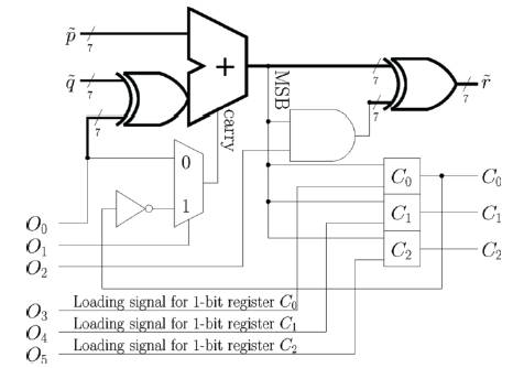
Figure 2. ACS unit
In this clock cycle the max* calculation is activated by using the operation code O=1011002 of Table II and loading operands p and q from the registers R1 and R2 .The result r is then stored in register R3,which is the approximated as |R1-R2|.The result C0 determines max(R1,R2).
The LUT comparison performed during the second ACS operation is activated by the operation code O=1100102 , operand p uses the constant decimal value 0.75, which is provided by the register bank1 in the architecture. Operand q take value from R3, which is the approximated |R1-R2|that was obtained in the previous clock cycle. In this clock cycle, the result r is not stored, while the result stored in C1 provides the outcome of the test |R1-R2|>0.75, as required by the second ACS operation.
Similar to the previous clock cycle, the result of the test|R1- R2|>0 or of the test|R1-R2|>2 is determined depending on whether it was previously decided that |R1- R2|>0.75.More specifically, we employ the operation code O=1100012 , which use the value stored in R3 for the ACS unit's operand q and substitute the constant value of 0 or 2 for p, as appropriate.
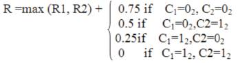
The max* calculation is completed in the fourth clock cycle by using the operation code O=0000002 .Here the operand p is provided by the maximum R1 and R2,as identified by C0.Meanwhile, a value for the operand q is selected from the set {0.75,0.5,0.25,0},depending on the contents of C1and C2.As a result, we have
Operation of ACS unit is shown in table1.
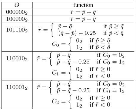
Table .1 Operation of ACS units
A flip flop does not need to be clocked with a free running clock. Clock gating is when you have some logic that then generates the clock to that flip flop as well as additional logic to generate the 'D' input to that flop as shown in Figure 3.When there is no activity at a register “data” input, there is no need to clock the register and hence the “clock” can be gated to switch it off. If the clock feeds a bank of registers, an “enable” signal can be used to gate the clock, and is called the “clock gating enable”. Here the power is reduced because it takes energy to switch any signal from one voltage level to another. By replacing a signal that is always toggling with one that only toggles when needed you are reducing the amount of energy used. Typically, clock gating can be used on printed circuit board designs and ASIC designs because in order to implement the design correctly one needs to have very good control of the minimum and maximum propagation delays. Inside an FPGA (Field Programmable Gate Array) you don't have this sort of control. So clock gating is not used very often and even less often is it used successfully.
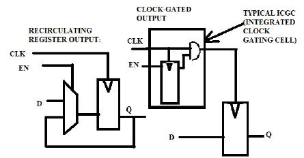
Figure 3. Clock gating
When an “explicit” clock enables exists in the RTL code, synthesis tools may choose between two possible implementations.
In the “re-circulating register” implementation the enable is used to either select a new data value or re-circulate the previous data value. In the “gated clock ”implementation, when the enable is off, the clock is disabled. The output of the two implementations will always be identical, but the timing and power behavior will be different clocks for the register and hence the “clock” can be gated to switch it off. If the clock feeds a bank of registers, an “enable” signal can be used to gate the clock, which is called the “clock gating enable”.
Before implementing clock gates, it is critical to make sure that all gating opportunities save power instead of increasing power. For example, if the clock enable is always high, inserting a clock gate and additional enable logic will consume more power. In addition to increasing power due to new enables, every time a clock gate is added to the clock tree it introduces an additional delay and makes clock tree synthesis more difficult. Just performing activity analysis is not enough to see if the new enables actually save power. Differential power computation is actually required to calculate the power savings after gating.
In Figure 4, when the signal from the turbo encoder to turbo decoder is received through the channel, the input data which given to the decoder setup and the clock pulses which are given to the decoder whose function is based on LUT-Log BCJR algorithm, decodes the data from the channel. The clock generator which generates the clock pulses and the clock divider setup which divides the clock signal to the turbo decoder setup. Clock gating involves the Gated clock signal. Gated clock is a wellknown method for reducing power consumption in synchronous digital circuits. By this method the clock signal is not applied to the flip flop when the circuit is in idle condition. This reduces the power consumption.
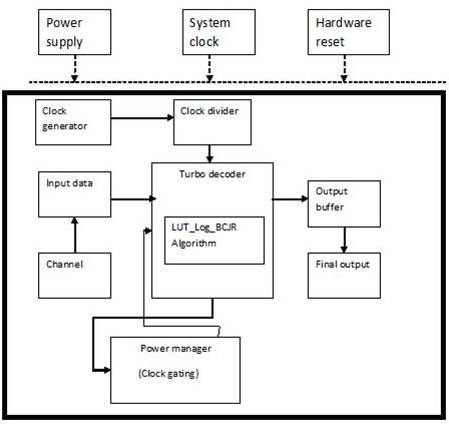
Figure 4. Proposed Architecture
In a digital circuit the power consumption can be accounted due to the following factors: Power consumed by combinatorial logic whose values are changing on each clock edge and Power consumed by flip-flops. Figure 5, shows that it contributes to most of the power usage. A flip flop consumes power whenever the applied clock signal changes, due to the charging and discharging of the capacitor. If the frequency of the clock is high then the power consumed is also high. Gated clock is a method to reduce this frequency.
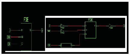
Figure 5. RTL Diagram Without Clock Gating
The clock is always applied to the flip flop and this results in considerable loss in power due to frequent charging and discharging of the capacitor. RTL diagram which is shown in Figure 6 involves the clock and load. Note the AND operation between load and clock signal. Here the clock to the flip flop "FD" is said to be gated. The code's purpose is that, the output has to change only when load is '1' at the rising edge of clock. So it is useless to drive the flip flop when the load signal is '0'.If the load signal changes very rarely, then the above gated clock code will result in a low power design.
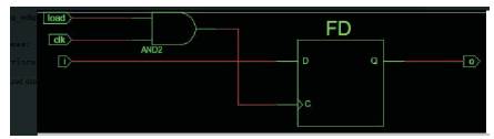
Figure 6. RTL diagram with clock gating
Clock gating is also termed as power manager because the power gets reduced through the clock gating on the decoder setup.
Figure 7 shows the simulation result of Turbo Encoder which involves analysis of the signal through the convolutional encoder setup of upper and lower encoder interleaver.
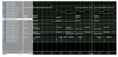
Figure 7. Simulation result for Turbo Encoder
Figure 8. shows the simulation result of Turbo decoder with clock gating technique which involves reduction of dynamic power consumption.
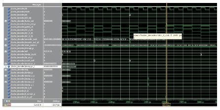
Figure 8. Simulation result for Turbo Decoder with Clock Gating
In this paper, a new approach of turbo decoder architecture has been designed, while the conventional LUT-Log-BCJR architecture consumes more energy and wasteful designs requiring high chip area. A motivated low complexity turbo decoder is designed with the decomposing of ACS unit with clock gating technique. This is simulated in the MODELSIM software. In future turbo decoder with clock gating will be implemented in FPGA using Xilinx.