(1)
Graphene Nanoribbons(GNR) and Carbon Nanotubes(CNT) represent a novel class of low-dimensional materials. These Graphene based nanostructures are used in wide range of nanoscience and nanotechnology applications. In this article, the performance potential of ballistic Graphene and Silicon Nanowire(SiNW) field effect transistors are examined for future high-performance applications. A thorough investigation has been made to realize the performance of these three types of transistors in terms of drain current, transconductance, number of mobile charge, quantum capacitance, gate capacitance, gate delay and cut off frequency using ballistic top of the barrier model. On-current, transconductance and gate capacitance control the switching speed of a transistor. It is shown that, the on-current in carbon based channel is higher as well as Ion/ioff is higher than SiNW channel due to lower effective mass. Higher oncurrent indicates sharper slope in current curve which ensures higher transconductance. It is also shown that the Density Of States(DOS) of CNT and GNR transistors are lower than the SiNW transistor. Through extensive computer simulation it is shown that the Graphene transistors can be the candidates for future digital switches. It is also important that SiNW transistors are potentially attractive and give the central role of silicon in the semiconductor industry and the existing set of known fabrication technologies.
In modern integrated circuit, it is observed that Metal Oxide Semiconductor Field Effect Transistor (MOSFET) channel length changes in nanometer scale. The Si transistor in production today is below the 100 nm scale and has entered the nanoelectronics regime. Over last decade continuous scaling of silicon transistors has been the driving engine for the exponential growth of digital information processing systems. Scaling limit in Si Fieldeffect Transistors (FETs) change on certain conditions [1]. The main reason for reducing the space size of transistors is to pack more devices in smaller area. Increased number of transistor in a chip causes better device performance. The cost per integrated circuits is mainly related to the number of chips that can be produced per wafer. More the chips are added in an IC, less is the cost [2].The number of transistors per chip has been doubled every 2–3 years once a new technology node is introduced over the past 30 years. This doubling of transistor density was first predicted by Gordon Moore in 1965 and is commonly referred to as Moore's Law [3].
Carbon Nanotubes can be considered as graphite sheets with a hexagonal lattice that has wrapped up into a seamless cylinder. Their electronic conductivity, for example, has been predicted to depend sensitively on tube diameter and wrapping angle with only slight differences in these parameters causing a shift from a metallic to a semiconducting state [4].The band gaps of both Metallic and Semiconducting Carbon Nanotube are consistent with theoretical predictions [5].From early Carbon Nanotube experiments, owing to their molecular uniformity and quasi-one dimensional natures, it was expected that they would exhibit ballistic transport properties. It shows that carbon nanotube exhibit low temperature transport effects such as Coulomb blockade. However, further research is still required to determine experimentally their role in nanotube devices [6]. An additional advantage of nanotubes is that their extended lengths facilitate the use of standard electron beam lithography for device fabrication. In a Carbon Nanotube the electrons are free to move only in the length direction [7].
Silicon Nanowires (SiNW) are the most perspective elements of Nanotechnology. SiNW can be used in nanoelectronics as field-effect transistors, diodes, logic gates, and more. The structure and properties of silicon nanowires and nanorods under high pressure is almost a virgin field [7].The best example of this is the vapor-liquidsolid mechanism of Si wire growth proposed by Wagner and Ellis in their seminal article published in March 1964 [8]. The Vapor-Liquid-Solid (VLS) growth mechanism is still the most prominent method for silicon wire synthesis [9]. Different techniques for silicon nanowire synthesis were developed with High Temperature Chemical Vapor Deposition, Low Temperature Chemical Vapor Deposition, Supercritical-Fluid-Based and Solution-Based Growth Techniques, Molecular Beam Epitaxy, Laser Ablation, Silicon Monoxide Evaporation etc [10-11].
Graphene allows enormous research since its experimental discovery in 2004. It consists of carbon atoms arranged in a 2-dimensional honeycomb crystal lattice with a bond length of 1.42 Å. Two types of Graphene Nanoribbons are found considering on edge shapes one is armchair GNR and another is zigzag GNR. Graphene sheets can be processed with conventional CMOS-technology is potentially a huge advantage over CNTs. Two-dimensional Graphene is a zero gap material, which does not suitable for transistor applications. Recent theoretical works have shown that Graphene Nanoribbons have an energy gap which has an oscillating behavior as a function of width, with average roughly proportional to the inverse width, and that edge states play a very important role in inhibiting the existence of fully Metallic Nanoribbons [12].The width of the ribbon and its transport orientation relative to the Graphene crystal structure are the two parameters that determine the band-gap and the electronic properties of the GNR in a similar way that the chirality controls the properties of the CNT [13].
A. Javey et al. investigated gate voltage, cut-off frequency and drain current for CNT and SBFET in early 2003 [14]. It was shown that, under ideal conditions the transfer characteristics for each device is identical. GNRFET has 50 % larger Ion (i.e. current for V G= V DD, V D= VDD ) and larger transconductance gm than the SBFET [14]. DD This observation agrees to a conclusion in a previous literature that the on current of a ballistic SBFET with positive Schottky barrier height is smaller than that of a ballistic MOSFET due to the tunneling barrier at the source end of the channel [15]. In the SiNW the quantum capacitance increases with the gate voltage under low gate bias (nondegenerate) while it decreases with the gate voltage under high gate bias (full-degenerate). The QC vs. GSV plots for the simulated SNWT with a SiO2 layer and a high-K insulator layer. When the gate insulator capacitance is significantly larger than the Quantum Capacitance, the FET works at the Quantum Capacitance Limit (QCL) – the potential at the top of the barrier is insensitive to the local electron charge, Q-top, and is solely determined by the applied voltage biases [16].
In this article, GNR FET, CNTFET and SiNWFET are investigated in terms of drain current I D, transconductance gm, number of mobile charge, Quantum Capacitance CQ, Gate Capacitance CG, gate delay τ and cut off frequency fTusing ballistic top of the barrier model. We also explored the role of GNRFET in future electronic system.
Scaling behavior in Graphene Nanoribbon has major changes compared with SI MOSFETs. Reducing the oxide thickness is more useful for improving transistor performance than using a high-κ gate insulator. When,the channel length scaled below 10 nm, a significant increase of the minimal leakage current is observed. This happens because small effective mass provides strong source drain tunneling. Scaling limit in Si MOSFETS is no longer followed in GNRFET. The intrinsic switching speed in GNR SBFET is several times faster than that of Si MOSFETs. And that could lead to promising high speed electronics applications in GNRFET where large number of leakage is no longer concerned. The total gate capacitance is limited by the semiconductor capacitance and it is no longer dependent on the gate insulator capacitance. The GNRFET has a one-dimensional channel with a monolayer of carbon atoms. It has small semiconductor capacitance which makes it to operate closer to the quantum capacitance limit compared with the Si FETs. The advantage to use multiple gate geometry is for the immunity to the short channel effects. A thinner oxide is therefore better for larger on current and on-off current ratio due to smaller sub threshold swing. Small size and low dimensional contacts not only improve the DC performance by increasing the on current, but also improve the AC performance by decreasing the parasitic capacitance between the electrodes, which leads to a higher operation speed [13].
GNR and CNT are one-dimensional Nanostructures and both derived from Graphene. The scaling characteristics of GNR SBFETs show some similarities with CNT SBFETs. But the two types of transistors have some important difference. First, GNRFETs have different channel geometry leading to a different gate electrostatics. And a precise patterning technique could potentially lead to better control of defining channel material than CNTFETs. Second, due to the different quantum confinement in the transverse direction, an armchair edge GNR channel does not have valley degeneracy [17], which results in a smaller quantum capacitance. Compared to a CNT channel, it benefits even less from multiple gate structure. In addition, the edges of the GNR channel could potentially cause large potential variation in the transverse direction. The band gap of the GNR channel strongly depends on its width, which significantly affects the on current and off current. The larger on current is found to reduce the gate insulator thickness and contact size results in thinner Schottky barriers. The intrinsic speed of the GNRFETs is several times faster than Si FETs due to its large carrier velocity and near ballistic transport, and reducing the parasitic capacitance results fast intrinsic speed [18]
The model takes the band structures of GNRs as an input and it has previously been applied to model silicon nanoscale MOSFETs, nanowire FETs, and CNTFETs. This model provides insights into the performance of MOSFETs near the scaling limit, and a unified framework for assessing and comparing a variety of novel transistors. The model assesses the performance limits by assuming (i) the channel is ballistic (no scattering), and (ii) the transistor contacts are ideal (with a perfect transmission).To derive the top of the barrier model we are following theoretical issues that are provided in Fundamentals of Nanotechnology course. Related issues are given below,
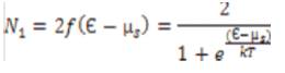
A single energy model of a ToyFET includes the contactdevice coupling and then extend it to the single sub-band model (Figure 1). The ToyFET model was originally proposed by Prof. Supriyo Datta of Purdue University to understand the transport mechanism of molecular transistors. Let us consider a simple picture shown below. The device part is represented by a single energy level Є. The source contact is characterized by a Fermi level µsand the drain contact by µd. At equilibrium, both the source d and drain Fermi levels align and therefore no current flows. Now if we apply a drain bias then µs - µd=Vds and an energy window is created for current to flow. However, if the energy level of Є is not between µs and µd then no current will flow. Under that situation, we have to apply the gate bias to bring the energy level Є in the energy range between µs and µd for the current to flow. Now the source contact will inject electron and try to fill the energy level Є and the drain contact will try to empty it out. Therefore, a balance between filling up and emptying out will be established and current will flow. If N1 is the average number of electrons that the left contact would like to see at the channel then [19].
Here the factor of 2 includes spin degeneracy. Similarly the average number of electrons N2 that the drain contact would like to see at the channel is[19]
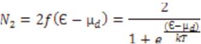
However, the average number of electrons at the channel is N at stead-state. Therefore, N1 -N is the average number of electrons that are pumped into channel from the source contact.
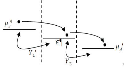
Figure 1. Fermi Energy level in ToyFET
The transport in most of the Nanostructures such as Carbon Nanotubes, silicon nanowires is ballistic in the ultimate scaling limit. The ballistic current has both the tunneling and the thermionic components. Here an analytical model is derived for the I-V characteristics of Nano-devices under single sub-band approximation. The current is thermionic only in the derivation. The Landaur equation for ballistic current is[19]
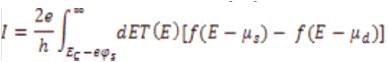
where,e is the electron charge, h is Planck's constant, T(E) is the transmission coefficient, f is the Fermi distribution function, µs and µdare the source and drain Fermi levels, respectively, and the factor of 2 accounts for spin degeneracy. The integration is performed from the bottom of conduction band to infinity for electron current.The conduction band bottom without gate bias is Ec and φs is the surface potential. For thermionic emission current T(E)=1, the current can be simplified as [19].
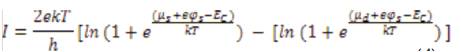
where, and
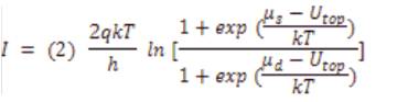
and  .The first term in the expression of current is the forward term that dominates in the saturation and the second term is the backward term that dominates in the linear region, for undoped channel with reference energy EF =0. Eq. (4) can be further simplified for sub-band degeneracy as [19].
In the derivation of current, the quantity φs is called surface potential. The current expression is derived assuming a single point as the channel, where the potential barrier along the source to drain is highest, and the transmission coefficient is unity above it and zero below it. This point of the channel is electro-statically connected to the gate, to the source, and to the drain that can be schematically represented as shown in Figure 2.
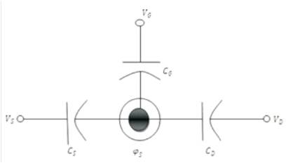
Figure 2. The potential at the top of the barrier is controlled by the gate, drain, and source potentials through the three capacitors
Now the expression of charge above equilibrium at that channel point would be balanced by the charge associated with the three capacitors as follows[20]

 is the gate control parameter, αs =
 and αd = and
 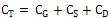 is the total capacitance. The term
  is related to the quantum capacitance. When a device operates in the quantum capacitance limit, then αg becomes unity and αs=αd=0.To calculate the surface potential N = N at equilibrium i.e φS=0).The 0 total number of electron can be obtained by integrating the DOS function times the quasi Fermi function in energy. However, we do not know the quasi Fermi function in the channel; rather we know the two Fermi levels, mand m s d How the channel states are populated by the carriers according to thes two Fermi levels are shown in Figure. 3.
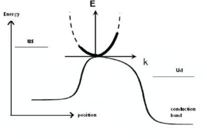
Figure 3. k states at the top of the barrier insert by two Fermi level
The electrons that are injected from the left (source) contact have positive velocity.Therefore, the right half(positive k) of E-k relation will be filled up by the carriers according to the source Fermi level. Similarly the left moving electrons will fill up the negative k states according to the drain Fermi level. Now if we approximate the local density of states by bulk expression, then half of the bulk DOS will be associated with the source and next half with the drain (E-k is symmetric).However, at equilibrium the two Fermi levels are equal (Ef) and N0 can be obtained from,
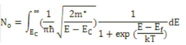
It should be noted that Eq. (7) does not contain channel length L, because we are calculating the density of electrons not the actual number of electrons. Now the positive moving electrons N+ and the negative moving N- electrons can separately be calculated according to Eq. (8) and N = N+ + N-
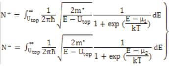
where we use 
This research involves simulation study to investigate the IV characteristic of Graphene and Silicon Nanowire transistors. The simulation is carried out on single subband top of the barrier model [14]. Three kinds of devices have been investigated for their performance based on a common off-current. The ballistic top of the barrier model is used to evaluate the current voltage characteristics. Finally, the results are interpreted and conclusions are drawn based on the obtained results. The model takes the band structures and the effective mass as inputs. The model assesses the performance limits by assuming (i) the channel is ballistic (no scattering), and (ii) the transistor contacts are ideal (with a perfect transmission). Therefore, upon comparing GNR, CNT and SiNW devices, factors such as the bandgap and the fact that a certain diameter CNT has a larger conducting circumference than a GNR of the same width should be taken into consideration. In all simulations, off-current is set to 10nA and the thickness of high-k dielectric material is 3 nm to increase the gate capacitance [15]. So in this work, we compare a GNR having a width close to the circumference of the 1.5 nm CNT and SiNW. The parameters used for simulation are listed in Table 1. The parameters of Table 1 are taken from FETToy parameters,and those values are constant for ultra-short gate channel which channel length is 1 nm.
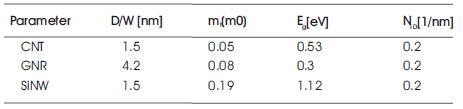
Table 1. List of parameters used in simulation
Figures 4 and 5 show the drain current versus (ID) gate bias (VGS) plots for a drain bias of 0.5V. In these characteristics, VGS=0 is corresponding to a drain current of 10nA. As VGS shown in Figure 1 and Figure 5, the on current of wider GNR show a slight improvement against the SiNW which has the same diameter as CNT. It has been observed that ID versus VGS curve for each transistor. In Figure 4, the on- current of CNT, GNR and SiNW are 35.1μA, 32.6μA and 28.3μA respectively. The higher on-current in carbon based channel is due to lower electron effective mass. Recall that off-current is common for every transistor, so ION/IOFF of GNR is less than CNT but greater than SiNW.
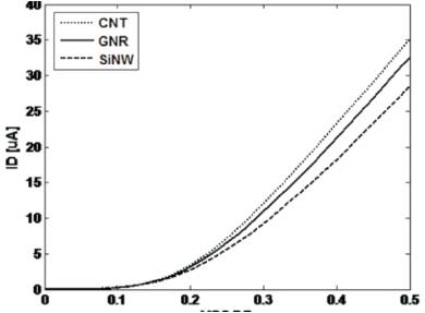
Figure 4. ID versus VGS characteristics of three types of transistors at VDS =0.5V
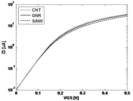
Figure 5. ID versus VGS characteristics of three types of transistors at VDS=0.5V
Figure 6 shows the transconductance versus gate bias plots for a drain bias of 0.5V. From Figure 3 it has been observed that at VON the magnitude of transconductance of CNT, GNR and SiNW transistors are 0.121mS, 0.115mS and 0.107mS. So the transconductance of CNT transistor is higher than GNR transistor and the transconductance of GNR transistor is higher than SiNW transistor.
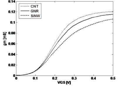
Figure 6. gm versus VGS characteristics of three types of transistors at VDS =0.5V
Figure 7 shows the number of mobile charge versus gate bias plots for a drain bias of 0.5V and VGS =0 is corresponding to a drain current of 10nA. In Figure.6-7, at VON the number of mobile charge of CNT, GNR and SiNW transistors are 3.5×106cm-1 , 4.2×106cm-1 and -1 6.1×106cm-1. The reason behind the better performance of GNR and CNT transistors than SiNW transistor is shown in Figure 7. The effective mass of CNT is lighter than GNR and the effective mass of GNR is lighter than SiNW and from the equation of Density-Of-States (DOS) it is known that DOS is directly proportional to the square root of effective mass of electron. Higher DOS of SiNW provides higher channel charge density.
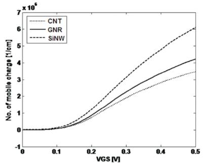
Figure 7. No. of mobile charge versus VGS characteristics of three types of transistor at VDS =0.5V
Figure 8 shows the quantum capacitance versus gate bias plots for a drain bias of 0.5V. In this figure, VGS =0 is corresponding to a drain current of 10nA. From Figure 8 it is clear that SiNW has higher quantum capacitance than GNR transistor, and GNR transistor has higher quantum capacitance than CNT transistor. Small quantum capacitance is an important requirement for effective gate control of transistors. The quantum capacitance is proportional to the DOS at Fermi energy. As CNT has the lowest DOS due to the lightest effective mass, its quantum capacitance is the least and that of SiNW is the highest. In Figure 8, the peak value of quantum capacitance of SiNW, GNR and CNT transistors are 5.6pF/cm, 3.6pF/cm and 2.8pF/cm. Figure 8 shows that when VGS increases from 0, energy of the top of the barrier decreases, so the top of the barrier gets close to Fermi level and that's why quantum capacitance increases. This condition is valid until the energy of top of the barrier is greater than Fermi energy. When Fermi energy is equal to the top of the barrier energy, then the quantum capacitance reaches to its peak value. Again when top of the barrier energy is less than Fermi energy and still decreases by increasing VGS then quantum capacitance decreases slowly.
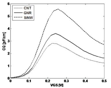
Figure 8. Quantum capacitance versus VGS characteristics of three types of transistors at VDS =0.5V
Figure 9 shows the gate capacitance versus gate bias plots for a drain bias of 0.5V and VGS =0 is corresponding to a drain current of 10nA. Here COX is constant but depends on channel material and shape. Quantum capacitance is in the series of COX and CQ . So CG is primarily controlled by CQ , because of small CQ the series combination of CQ and COX is less than CQ ,and so by comparing Figure 8 and Figure 9, it is being observed that the total gate capacitance decreases almost 45% than quantum capacitance. From Figure 9, the peak values of gate capacitance of SiNW, GNR and CNT transistors are 3.5pF/cm, 2.3pF/cm and 2pF/cm.
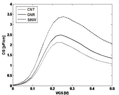
Figure 9. Gate capacitance versus VGS characteristics of three types of transistor at VDS =0.5V
Figure 10 shows the gate delay versus gate bias plots for a drain bias of 0.5V and VGS =0 V is corresponding to a drain current of 10nA. As we know the lower the value of gate delay, the more effective the FET becomes as a switch. Gate delay is directly proportional to the gate capacitance and inversely proportional to the on-current. On-current is individually constant for different types of transistors which are shown in Figure 3. So to achieve low gate delay it is necessary to have high on-current and low gate capacitance. From Figure 10, the peak values of gate delay of SiNW, GNR and CNT transistors are 5.93fs/nm, 3.83fs/nm and 3fs/nm.
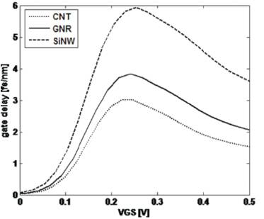
Figure 10. Gate delay versus VGS characteristics of three types of transistors at VDs =0.5V
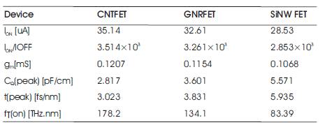
Table 1. Simulated values of I , I /I , gm, ON ON OFF CQ, τ , and fT of three types of transistors.
Figure. 11 shows the cut-off frequency versus gate bias plots for a drain bias of 0.5V and VGS=0 is corresponding to a drain current of 10nA. Cut-off frequency is an important performance metric for high frequency performance of a transistor. It is known that the cut-off frequency is directly proportional to the transconductance and inversely proportional to the gate capacitance [19], and we also know that higher the cut-off frequency, the more effective the FET becomes as a switch. So to achieve good amplifier response from a transistor it is necessary to have high transconductance. In Figure 11, it is shown that the cut-off frequency of CNT, GNR and SiNW transistors are 178.2THz nm, 134.1THZ nm and 83.4THz nm.Single-walled CNTs, GNR and SiNW have intrinsic cutoff frequencies approaching the THz range.
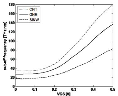
Figure 11. Cut-off frequency versus VGScharacteristics of three types of transistors at VDS =0.5V
The performance comparison of Carbon Nanotube, Graphene Nanoribbon and Silicon Nanowire transistors are studied along with the I-V characteristics of Carbon Nanotube, Graphene Nanoribbon, and Silicon Nanowire transistors. Also are simulated the characteristics of transconductance, number of mobile charges, cut-off frequency, and quantum capacitance and gate capacitance. For every simulation a common off-current 10nA. is fixed. It gives better performance in CNT transistor compared to GNR and SiNW transistors. It has been observed that CNT got higher on-current than GNR. And SiNW got almost lower on-current compared with GNR. So ION/IOFF ratio of GNR must be higher than SiNW but lower than CNT. At on state CNT transistor shows low mobile charge compared to the SiNW transistor. CNT transistor contains small quantum capacitance compared to GNR transistor. And SiNW transistor got higher quantum capacitance than CNT transistor. For SiNW top of the barrier gets closer to the Fermi level so in this way quantum capacitance increases. And for CNT top of the barrier got away from the Fermi energy so that quantum capacitance decreases slowly. here the cut-off frequency of CNT transistor is higher than GNR transistor. Lower gate delay exhibits faster performance in different transistors, as we have got low gate delay for GNR transistor compared to SiNW transistor and CNT transistor shows lower gate delay than GNR transistor. We consider CNT transistor is good amplifier compared to GNR and SiNW transistors by showing higher frequency performance and higher transconductance. Investigating GNRFET, CNTFET and SiNWFET characteristics are very interesting since the device has many aspects that can be explored and improved.