(1)
In this paper, a highly durable Double Edge Triggered D-Flip Flop based Serial in Serial Out (SISO), Serial in Parallel Out (SIPO), Parallel In Serial Out (PISO) and Parallel In Parallel Out (PIPO) shift registers are designed using 10nM Carbon Nano Tube Field Effect Transistor (CNTFET) technology. The CNTFET is a cutting edge device to overcome the current CMOS technology for its excellent electrical properties. To evaluate the durability, shift registers using CNTFET are analysed and the transient analysis are depicted. Power consumption, delay, PDP, rise time and fall time are evaluated using HSPICE with 1GHz operating frequency.
The major challenges of the semiconductor industry at the nanoscale are: (1) performance and power optimization (2) control of variations at the nanoscale and device fabrication and (3) integration of numbers of devices on to a same chip. Nanotechnology has been put forward as the key to meeting many challenges of the industry. New physical phenomenon and synthesis techniques are being studied. While there have been significant advancements in scientific discovery at the nanoscale, the engineering work that makes the science into manufacturable technologies is just in initial stage. In this paper, we focus on the use of the carbon nanotube transistor as an element for designing digital circuits. While very promising experimental results have been published in recent years, in order to develop a new transistor into an acceptable technology, an engineering approach needs to be adopted. We need to develop the appropriate device models and design tools with different level of abstraction to enable the design of a VLSI system. This is distinct from the science nature of determination and explanation of physical phenomena. Silicon based technology will reach its limits in 2020 when the channel length of MOSFET becomes less than 10nm.
CNTs have diameter of typically 1 to 3 nm, but being long up to several microns. CNTs can be exploited to build both low-resistance high-strength interconnections and highly scalable low-power Carbon Nanotube Field-Effect Transistors (CNTFET) and single electron tunnelling transistors[2]. Presently, many research teams carry out studies about CNTFET devices and their logic applications all over the world, both in industrial laboratories (IBM, Intel, Infineon) and in universities (Purdue and Stanford).
Power consumption is one of the crucial parameter of Very Large Scale Integration (VLSI) circuit design. The sources of power consumption in a digital CMOS circuits are:
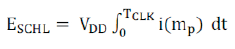
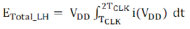
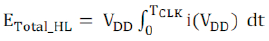
In digital CMOS circuits, when both pull up and pull down networks are in ON condition, then it exhibits a direct flow from VDD to ground, which results in short circuit power dissipation[3]. The short circuit energy for high to low transition and low to high transition are given by,
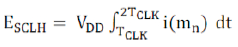
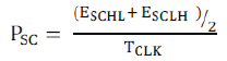
where, Tclk is the clock frequency.
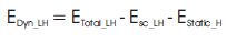
The static power of a CMOS circuit is the power dissipated during steady state conditions. For nanoscale VLSI circuits, the leakage current is due to mainly subthreshold voltage. Although dynamic power is dominant for technologies at 0.18μ and above, leakage (static) power consumption becomes another dominant factor for 0.13μ and below. One of the main contributors to static power consumption in CMOS is subthreshold leakage current[20] i.e., the drain to source current when the gate voltage is smaller than the transistor threshold voltage[4].
Power consumption is dominated by leakage power dissipation when the device dimension shrunk down to sub-22nm technology. The static power of a circuit can be found by measuring the leakage power during logic high input and logic low output with VSS as input and VDD as output respectively. [19]
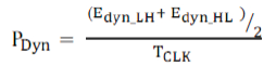
The power dissipation due to charging and discharging of the capacitance during transistor switching is said to be capacitance switching power. It falls under the category of dynamic power dissipation. It can be found by using the following energy relations.
where

where
Dynamic power due to capacitive switching can be measured by using (Pdyn):
This paper is organized as follows: Section 1 explains the Ballistic Carbon Nanotube Field Effect Transistor (CNTFET) model and their specifications. The DETFF and DETFF based Serial in Serial Out (SISO), Serial in Parallel Out (SIPO), Parallel In Serial Out (PISO) and Parallel In Parallel Out (PIPO) shift registers are explained in section 2. The transient analysis for DETFF, SISO, SIPO, PISO and PIPO shift registers using 10nm CNTFET model are depicted in section 3 and performance of DETFF, SISO, SIPO, PISO and PIPO shift registers using 10nm CNTFET model are evaluated in terms of average power, delay, PDP, rise time and fall time in Section 4. Paper ends with the conclusion.
The semiconductor industry is looking for alternate materials and devices to integrate with the current silicon-based technology - carbon nanotubes, along with silicon-germanium (SiGe) and Gallium Arsenide (GaAs) being the possible successors to overcome the hurdles. Carbon nanotubes (CNTs) are conductive/semi conductive, very small (just a few nanometres) and are capable of providing faster switching. Unlike graphene, which also has some special electrical properties, it is much simpler to create CNTs with semiconducting nature. Till now, the barrier for many research groups (such as IBM, Stanford) from building chips using carbon nanotubes is that it's very hard to produce pure form of semiconducting CNTs[6]. Depending on the rolling of graphene sheet, CNT can be either metallic or semiconducting and there is discovery has been made for large scale method of producing 100% semiconducting CNTs. Researchers only need the semiconducting variety, because the introduction of minute metallic CNTs will result in performance degradation of CNT transistors and will cause unpredictable electrical behaviour.[17]
The high electron and hole mobility (μ∼ 10, 000 cm2/Vs) of semiconductor nanotubes[8]; their compatibility with high-k gate dielectrics for coaxially-gated devices; the enhanced electrostatics and reduced short channel effects due to their molecular-scale diameters; and ability to readily form metal ohmic contacts make these miniaturized structures an ideal material for high performance, nanoscale transistors. CNTFETs use semiconducting single wall CNTs (SWCNTs) to assemble electronic systems; CNTFETs are having similar properties to that of MOSFETs. A single wall CNT consists of only one cylinder and the simple fabrication process of this device makes it a very promising alternative to today’s MOSFET. An SWCNT can act as either a conductor or a semiconductor, which depends on the angle of the atom arrangement along the tube[7].
The Carbon nanotubes were discovered by S. Ijiima in 1991 while doing some experiments on molecular structure composed of carbonium[11]. They can be considered as the result of folding graphite layers into carbon cylinders and may be composed of Single Wall Nanotubes (SWNTs) or multi-wall nanotubes (MWNTs) as shown in Figure 1. Depending on the folding angle and the diameter, nanotubes can be either metallic or semiconducting. The carbon nanotube is the foarth stable structure of carbon after diamond, graphite and fullerene[5]. An ideal nanotube can be thought of as a hexagonal network of carbon atoms (that form crystalline graphite) that has been rolled up to make a seamless cylinder. [19]
Figure 1. Arrangement of CNTs: a) Arm Chair, b) Zigzag & c) Chiral
Based on the chiral vector (the circular vector is perpendicular to the axis of the tube), Carbon nanotubes are classified into Arm Chair, Zigzag & Chiral as shown in Figure 1.
A CNFET is formed by a carbon nanotube connecting two metal electrodes on either side that form source and drain contacts, with gate electrode separated from the nanotube by a thin oxide film. Figure 2 shows ballistic CNTFET structure [1]. In 2003, the first experimental demonstration of the highly desirable metal ohmic contacts to the valence band of semiconductor SWNTs was reported, free of any barriers for holes by the use of high work function palladium (Pd) which also has a strong binding interaction with carbon nanotubes. [14]
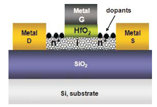
Figure 2. Ballistic Carbon Nano Tube Field Effect Transistor
Theoretical and experimental research has demonstrated the unique electrical features of CNTFET, including high transconductance and high ON/OFF current ratio[13]. The nearly ballistic transport at low bias implies the possibility of deriving carbon nanotube transistors. CNTFET could be more of an interest due to its similarities with MOSFET in terms of inherent electronic properties. Due to these similarities, previously designed CMOS architectures and basic CMOS based platforms can still be used without any major modifications.[12]
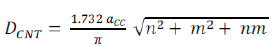
The diameter of CNT is given by
Thin films of high-k materials, such as ZrO2 and HfO2 (κ ~ 15–25), are highly desirable for gate dielectric integration in field effect transistors as they enable high ON-state current densities (speed) and low operating power consumptions.
The lack of dangling bonds at the nanotube/high-k interface and the weak non-covalent bonding interactions between the two materials, prevent any large perturbation of electron transport in carbon nanotubes. The integration of high-k dielectrics, however, has been a challenging problem towards many researchers in planar MOSFETs because of the inherent mobility degradation of the Si channels[16]. The thickness and dielectric constant of high-k material (Hfo2) are 4nm and 16 respectively. And the dielectric constant of silicon dioxide is 4.
The spacing between inner CNT’s is defined as pitch(s) and it is given by,
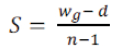
where,‘wg’ - width of the gate,
The parameters which are used in the model are shown in Table 1.
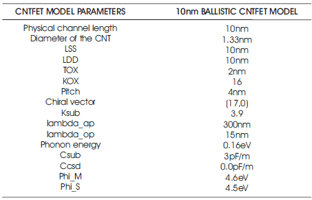
Table 1. Parameters of Ballistic CNTFET model
The parameters which are modified are briefly explained as follows.
The overall increase in current in our simulation can be justified by the physical explanation that the mean free path (A) is in general much longer than the channel length. The MFP of intrinsic CNT modelled for elastic scattering is ~ 200 nm, acoustic scattering ~ 500 nm, and optical phonon scattering ~ 15 nm [10].
CNTs are grown or transferred to a substrate using a fixed spacing (pitch) prior to defining CNTFET based gates and contacts. The channel region of CNT (below gate region) is undoped while the other regions of CNT are heavily doped; therefore they are acting as the source/drain extended region.
Theoretical studies have shown that a singlewalled CNT can be either metallic or semiconducting depending on its chirality and diameter. (n,m) nano tubes with n = m (armchair) are metallic; for n – m ≠ 3 × integer, the nano tubes are semiconducting. For n – m = 3 × integer, the nano tubes will be quasi-semiconducting with a small band gap. The sensitivity of CNT spectacular electrical properties on structural parameters opens up numerous opportunities in nano tube designs.
The diameter of the carbon nanotube is found to be 1.3502nm with acc=0.144nm (carbon-carbon bond length of graphene) and (17,0) for (n,m) chiral vector.
In order to establish the ultimate scaling limit imposed by source-drain tunnelling, very thin gate oxide (tox = 2nm for the channel length of 10nm and longer, and tox = 1nm for the channel length of 5nm) is used to ensure excellent gate controlled electrostatics. [9]
In digital circuits, a shift register is a cascading of flip flops, sharing the same clock, in which the output of each flip-flop is connected to the "data" input of the next flip-flop in the chain, resulting in a circuit that shifts by one position.
Compared to rising edge triggered flip-flop which process data only at the rising transition of the clock, the DET doubles the rate of data processing or, alternatively halves the clock rate thereby, either increasing the data throughput or reducing power consumption in the clock circuit respectively. Thus reduced power and high speed operation is possible [19]. One such high performance Double Edge Triggered D-Flip Flop is shown in Figure 3.
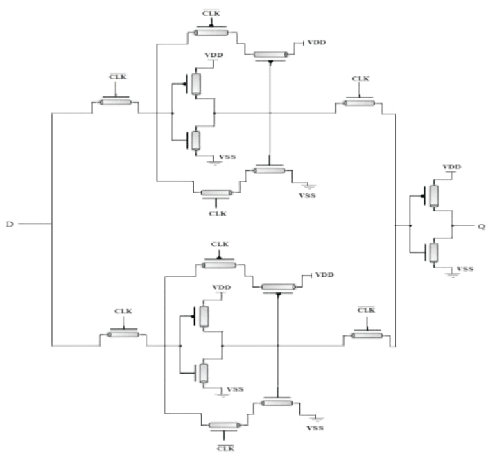
Figure 3. Highly Durable Double Edge Triggered D-Flip Flop
Basically, n-type pass transistors give weak high but in Figure 4, the n-type pass transistors are followed by an inverter, which results in strong high. Thus the High Performance DETFF in Figure 3 is free from threshold voltage loss problem of pass transistors. This Double Edge Triggered Flip-Flop (DETFF) is more efficient in terms of area, power and speed which claim for better performance than conventional designs.[15]
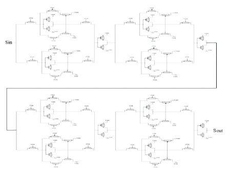
Figure 4. Serial In Serial Out Shift Register
Serial in serial out shift register accept data input serially on a single line and it gives the stored information on its output also in serial form. CNTFET based serial in and serial out shift register design is shown in Figure 4. Serial in parallel out shift register also accept data input in serial form. Once the input data is given, it may be either read off at each output simultaneously, or it can be shifted out and replaced. This configuration allows conversion from serial to parallel format. CNTFET based Serial in parallel out shift register design is shown in Figure 5.
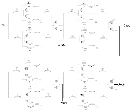
Figure 5. Serial In Parallel Out Shift Register
Parallel in Serial out Shift Register configuration has the data input on lines d1 through d4 in parallel form. To write the data to the register, the write/shift control line should be held low. To shift the data, the write/shift control line is brought high and the registers are clocked. Figure 6 arrangement shows CNTFET based design of PISO shift register. For parallel in parallel out shift register, all data bits occur as parallel outputs immediately following the simultaneous entry of the data bits with respect to clock. The circuit design of parallel in parallel out shift register constructed by CNTFET based proposed DET D flip-flops is shown in Figure 7.
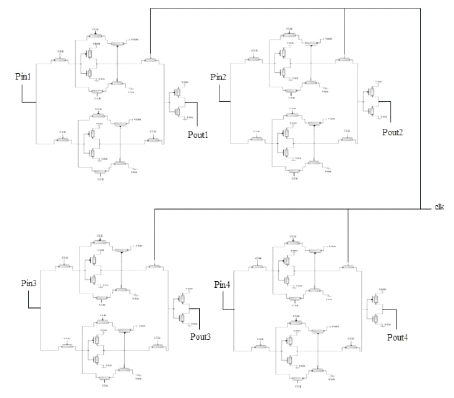
Figure 6. Parallel In Parallel Out Shift Register
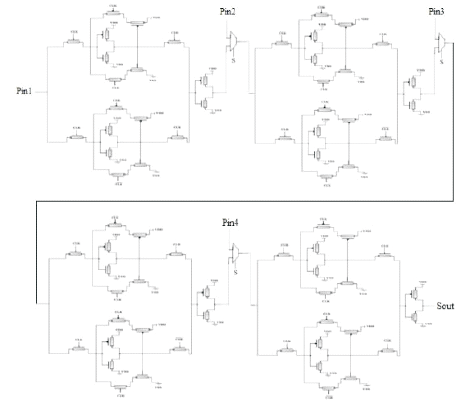
Figure 7. Parallel In Serial Out Shift Register
To evaluate the performance, the high performance DETFF based shift registers are designed using 10nm CNTFET. All simulations are carried out using HSPICE simulation tool at with 1GHz operating frequency. The simulated waveform of the high performance DETFF and shift registers using CNTFET are shown in Figures 8, 9, 10, 11 and 12.
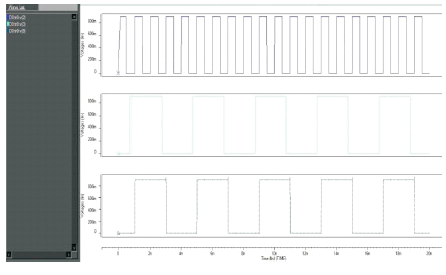
Figure 8. Transient Analysis of DETFF using 10nm CNTFET
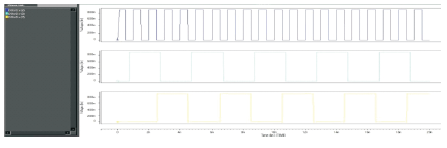
Figure 9. Transient Analysis of DETFF based SISO Shift Register using 10nm CNTFET
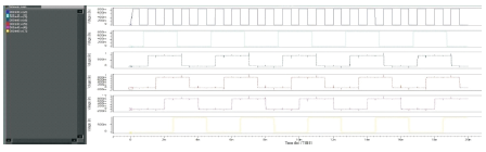
Figure 10. Transient Analysis of DETFF based SIPO Shift Register using 10nm CNTFET
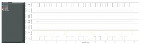
Figure 11. Transient Analysis of DETFF based PISO Shift Register using 10nm CNTFET
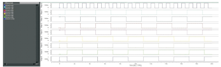
Figure 12. Transient Analysis of DETFF based PIPO Shift Register using 10nm CNTFET
The performance of the DETFF and shift registers using 32nm and 10nm CNTFET are evaluated by measuring the average power, delay, PDP, rise time and fall time and are furnished in the following Tables 2, 3, 4 and 5.
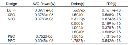
Table 2. DETFF and Shift Registers using 32nm CNTFET Technology
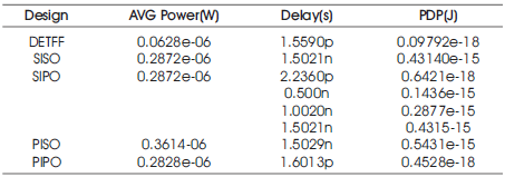
Table 3. DETFF and Shift Registers using 10nm CNTFET Technology
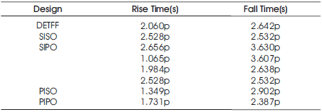
Table 4. Rise time and fall time using 32nm CNTFET Technology
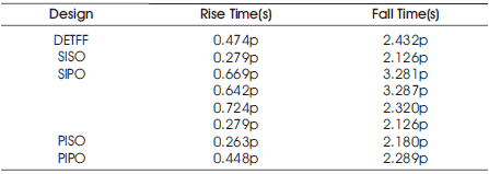
Table 5. Rise time and fall time using 10nm CNTFET Technology
Figure. 13, 14, 15, 16 and 17 show the power, delay, power delay product, rise time and fall time analysis of 32nm and 10nm CNTFET designs respectively.
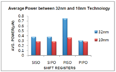
Figure 13. Average Power Analysis of 32nm and 10nm Technology using CNTFET design
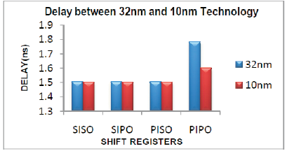
Figure 14. Delay Analysis of 32nm and 10nm Technology using CNTFET design
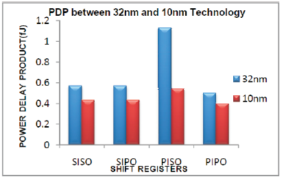
Figure 15. Power Delay Product Analysis of 32nm and 10nm Technology using CNTFET design
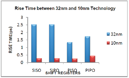
Figure 16. Rise Time Analysis of 32nm and 10nm Technology using CNTFET design
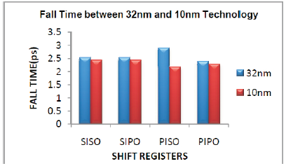
Figure 17. Fall Time Analysis of 32nm and 10nm Technology using CNTFET design
In this paper, we have designed a highly durable Double edge triggered D-flip flop based Serial In Serial Out (SISO), Serial In Parallel Out (SIPO), Parallel In Serial Out (PISO) and Parallel In Parallel Out (PIPO) shift registers using 10nm CNTFET technology. We have made a performance analysis on DET-FF and shift registers for exploring the average power, delay, PDP, rise time and fall which are useful for high performance and low power applications. In future, processors will be using CNTFET as its main core which will be more reliable and efficient than any other device yet existing in the field of electronics.