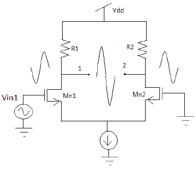
Figure 1. Single-Ended Differential Amplifier
A differential amplifier is an amplifier that amplifies the difference between two voltages and rejects the average or common mode value of the two voltages. The paper presented here is a single input - balanced output cascoded differential amplifier that amplifies a very small signal from the range of nV up to mV with a gain of 46.02db and operating with a constant gain upto 3MHz bandwidth. This work mainly aims at the amplification of very small input voltage and reduction of overall circuit power dissipation maintaining its linearity. Its application is for lower frequency and very small signal amplification. The total circuit power dissipation is only 32.3uW which is appreciably low. The circuit gain is 200 and it is operated with only 1V. The allowable input peak voltage is from 1nV up to 0.7mV and the output swing without distortion is 280mV peak to peak. For low frequency and low signal amplification this small signal amplifier with low power dissipation can lengthen the lifetime of a chip in IC technology which is powered by battery, if the total power dissipation is low.
The single-ended CMOS differential amplifier with active load is one of the most popular circuits used in analog and mixed signal circuits for signal processing applications, due to its good performance in terms of the common-mode rejection and voltage gain, combined with an extremely simple circuit structure, which performs directly differential to single-ended conversion. A phase splitter provides two outputs from a single input. These two outputs are 180 degrees out of phase with each other. The single-input, differential-output, differential amplifier will do the same operation. Figure 1 shows a differential amplifier with one input (at the Gate of M1) and two outputs (the Drain of M1 and M2). One output is in phase with the input signal, and the other output is 180 degrees out of phase with the input signal. The outputs are differential outputs. One further point of interest about this configuration is that if a combined output signal is taken between outputs number one and two, and this single output will be twice the amplitude of the individual outputs [1] [3] [6]. In other words, it will double the gain of the differential amplifier (single output) by taking the output signal between the two output terminals. This single-output signal will be in phase with the input signal. Much work has been reported by different researchers with high voltage supply to improve its performance in terms of its linearity, high gain, large bandwidth and constant transconductance but at the cost of higher circuit power dissipation [2] [4] [7] [5]. But this paper is presented for ultra low signal amplification with low power dissipation maintaining a high linearity for very low signal application.
Figure 1. Single-Ended Differential Amplifier
The gain of small signal in differential pair with current source load is relatively low and it is about 10 to 20 in submicron technologies. In order to increase the voltage gain substantially we increase the output impedance of both PMOS and NMOS devices by cascoding it as shown in Figure 2. In order to calculate the voltage gain the concept of half circuit is used, [1] as shown in Figure 3. Thus the gain is given as,
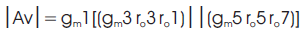
Where gms are the transconductance and ros are the output impedance of the devices.
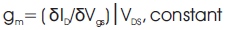
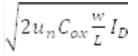
Transconductance represent the sensitivity of the device. Thus for high conductance, a small change in gate to source voltage results in large change in drain current. To obtain large conductance the ratio of (W/L) is increased. From small signal analysis ro is a linear resistor tied between drain to source. This output resistance have a large impact on many analog circuits and it is one of the limiting factors of voltage gain in CMOS amplifier circuit [1].
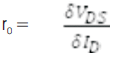
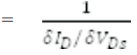
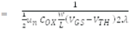

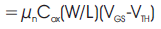
Where λ is channel length modulation which varies in length with the relative variation in VDS. Equations (4) and (7) shows that both output resistance and transconductance are dependent on (W/L) ratio by keeping other terms i.e overdrive voltage, mobility, oxide capacitance and channel length modulation constant. For high gain ro is increased by decreasing (W/L) ratio of the device which in turn decreases transconductance. The trade off between gm and ro can be compromised by optimising the aspect ratio (W/L) for high gain. For the circuit, the total gain is shown in Figure 4 i.e. the gain is twice the gain of half circuit as the mode of obtaining the output is balanced output.
Where AV is gain of half circuit.
Simulation is carried out for input voltage Vin1 at 5uV, 0.05mV and 0.7mV peak voltages operating at a frequency of 1 MHz. The amplified output voltage is obtained across out2 and out1 which is in phase with input voltage. The bias voltage is of 0.6 V with a tail current of 32.3uA. All the simulation results are shown in Figures 5, 6, and 7 respectively for input voltage 5uV, 0.05mV and 0.7mV.
The CMRR is relatively very high enough and approaches the ideal value as shown in the simulation result in Figure 8. For common mode input to both Mn1 and Mn2 the output is zero.
The circuit perform well up to 3MHz with a constant gain of 200 i.e. 46.02 db. After 3 MHz the circuit gain decreases as shown in Figure 8.
For nv input voltage range upto 0.7 mV the circuit maintain a high linearity as shown in the linearity graph. The maximum allowable output swing without distortion is 700mV but with a decrease gain. Figure 9 gives the circuit performance and Figure 10 shows the frequency response.Figure11 depicts the circuit linearity performance. Upto input voltage of 0.7mV the circuit maintains its high linearity but after 0.7mV the output deviates from its linear character as shown in Figure11.
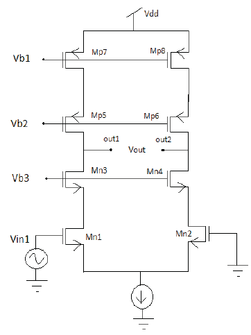
Figure 2. Transistor Level Cascaded Differential Amplifier with Single Input and Balance Output
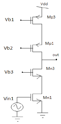
Figure 3. Half Circuit Concept
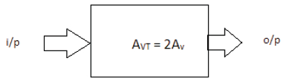
Figure 4. Total Circuit Gain is Twice the Gain of Half Circuit
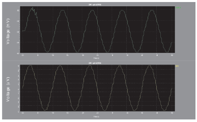
Figure 5. i/p Vol of 5uV Give o/p Vol of 1mV
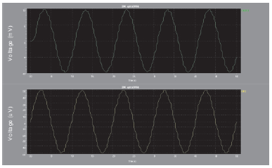
Figure 6. i/p Vol of 0.05mV Give o/p Vol of 10mV
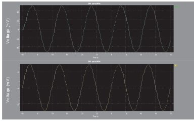
Figure 7. i/p Vol of 0.7mV Give o/p Vol of 140mV
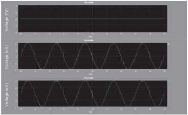
Figure 8. For Common Mode i/p, o/p is Zero
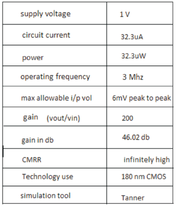
Figure 9. Circuit Performance
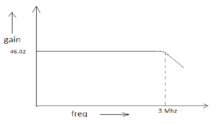
Figure 10. Frequency Response
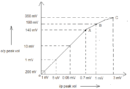
Figure 11. Linearity Graph
This circuit works linearly for peak input voltages from 1nV up to 0.7 mV with a constant gain of 200. When the peak input voltages exceed 0.7 mV, the output is still undistorted but the gain decreases and becomes no longer linear. Maximum peak input voltage for undistorted output is 3mV. The operating frequency bandwidth can be increased as high as 7 MHz by increasing the tail current but at the cost of higher power consumption. The CMRR of this work is also infinitely high with a low power consumption of 32.3 uW. All the design circuit performance are also tabled as shown in Figure 9 along with its linearity graph.