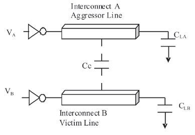
Figure 1(a). Driver and Aggressor Interconnect Lines
Crosstalk between interconnects is simulated by SPICE and the results are analyzed. The analysis shows that crosstalk between interconnects can be controlled by repeater insertion and proper sizing of the repeaters. For the best control of crosstalk smallest size repeaters with a number of repeaters is suggested. The dependence of cross-talk on signal transition time and interconnect length are examined and verified with previously reported results. Distributed RLC transmission line model of interconnect is considered.
In deep submicron technologies, interconnections in VLSI circuits are attaining appreciable lengths. The global on-chip interconnects are the major determinant of the cost, performance, energy consumption, reliability, and design complexity of VLSI systems. The international technology roadmaps for semiconductors indicate that the future nanometer scale circuits will contain more than a billion transistors and operate at frequencies above giga Hertz range [1]. Subsequently, the interconnect lengths have enhanced by several orders [2]. The long interconnect have parasitic resistance, inductance and capacitance associated with them in the VLSI chips, which are responsible for high delay in long interconnects [3-5]. Repeater insertion is an effective technique to mitigate delay[6-8]. Furthermore, in the present day VLSI-chips, proximity of interconnect induces serious cross-talk between the lines. Hence, a vital concern for the design of such circuits is to accurately model the electrical parameters of the lines keeping other issues like delay and power dissipation in mind as well [9-10]. Cross-talk is defined as unwanted coupling from neighboring signal wire to a network node that introduces interference. The resulting disturbance acts as a noise source and can lead to hard to trace intermittent errors, since the injected noise depends upon the transient value of the other signals routed in neighborhood. In integrated circuits, this inter signal coupling can be both capacitive and inductive [12]. It is seen that in repeater inserted interconnects the cross-talk depends on transition time and interconnect length [13-16]. However, the effect of repeater sizing on cross-talk is also an important parameter and research is still wanting in this area. Therefore in the present work simulation based analysis to find out the effects of repeater sizing on cross-talk is proposed.
The paper is organized as follows. In Section 1, cross-talk noise in interconnect lines is studied. In section 2, effect of repeater size variation on cross-talk in coupled interconnects for 130nm, 100nm and 70nm is presented. Lastly, the main conclusions of the present work are given.
Figure 1(a) shows the typical aggressor-victim model for interconnects [17]. Cross-talk between such lines greatly depends on line length and transition times of signals propagating down the interacting lines. We have used a simulation setup which is very much similar to the one used in [17]. All transistors are of channel length 130nm. For minimum size repeater L= 2λ and Wn=3λ and Wp= 2.5Wn, where L, λ, Wn, Wp are channel length, technology feature size, width of the n-channel and width of the p-channel MOSFETs respectively. A 130nm technology with copper interconnects process (SPICE MOS Models, 2007) [18] is used. The power supply (VDD) is kept at 1.5V. Each line of the coupled interconnect is 2mm wide, 0.68mm thick and separated by a spacing of 0.24mm. A distributed RLC model of interconnect is used. Each interconnect is modeled by 20 distributed lumps as shown in Figure 1(b). where section 1 is one such lump. The capacitance and inductance values are obtained using the mathematical model presented in reference [19]. Capacitive coupling has been considered between the two interconnect lines in this analysis.
Figure 1(a). Driver and Aggressor Interconnect Lines
Cross-talk noise for time varying from 1 to 25ps is investigated. These parameters are varied for four different cases of excitations to aggressor and victim lines.
The simulation set up measures maximum and minimum level of voltage magnitude at three nodes, viz, input of transmission line in2, output of transmission line out2 and at load capacitance of receiver Vout2 as shown in Figure 1(b). The results of the simulation regarding influence of aggressor signal transition time are shown in Figures 2-5 and are in agreement with those in [15].
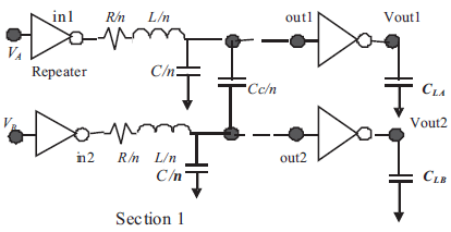
Figure 1(b). Interconnect Equivalent Model
The induced overshoot and undershoot can propagate false switching and can create a logic error. For the driver inverter, overshoot can cause negative conductance for PMOS and high electric field for NMOS. Furthermore, both overshoot and undershoot become significant with faster rise and fall times.
It is well known that with repeater insertion, delay [6] [7] [11] decreases and power dissipation increases. In this section the effect of repeater insertion and variation of repeater size on cross-talk is considered. In the interconnect model considered, the values of resistance, self capacitance, mutual capacitance and inductance are 1kΩ, 0.664pF, 0.334pF and 100nH respectively. Two coupled lines, one with repeater inserted and switching low to high and the other without any repeater inserted and at a static low voltage are considered. An RLC model of this system is shown in Figure 6.
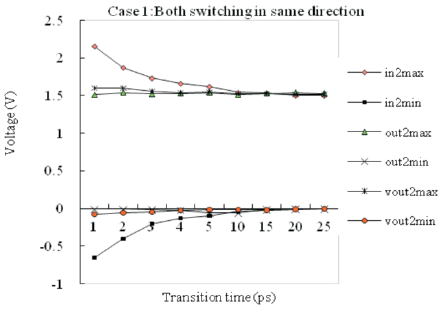
Figure 2. Variation of Node Voltage with Transition Time for 5mm Interconnect Line (case-1)
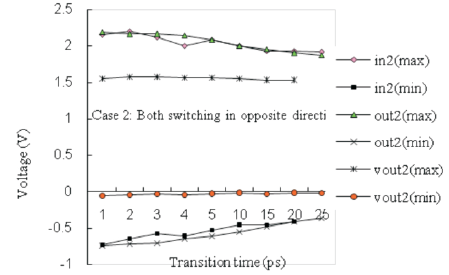
Figure 3. Transition Time vs Node Voltage for Interconnect Length of 5mm (case-2)
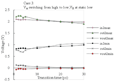
Figure 4. Transition Time vs Node Voltage for Interconnect Length of 5mm (case-3)
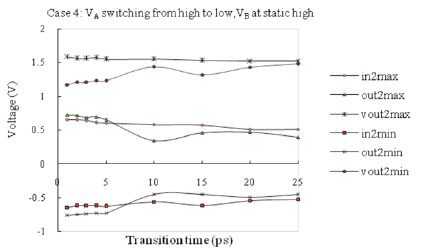
Figure 5. Node Voltage Variation with Transition Time for Interconnect Length of 5mm (Case-4)
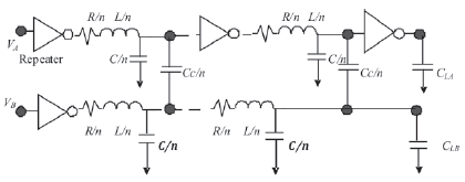
Figure 6. Coupled Interconnect Lines with Repeater Insertion in Line 1
As the size of the repeater increases the capacitance increases, the resistance associated decreases and hence current driving capability increase. Figure 7, shows the impact of repeater insertion on delay, power dissipation and cross-talk. The minimum size repeater has dimensions of Wn= 0.18µm, Wp=0.45µm and Ln = Lp = 0.13µm, for 130nm technology node. The basic principle of interconnect delay minimization is equalization of repeater delay and interconnect delay. Figure 7, implies that initially the interconnect delay dominates, becomes minimum for optimal number of repeaters and when the number of repeaters exceed the optimum value the delay due to inserted repeater is relatively more effective. Power increases with number of repeaters. Cross-talk reduces as the number of repeaters is increased. In the present work, the prime aim has been to investigate the effect of variation of repeater size on cross-talk. Figure 8 shows the variation of cross-talk in a repeater inserted interconnect line for different repeater sizes for 130nm technology node.
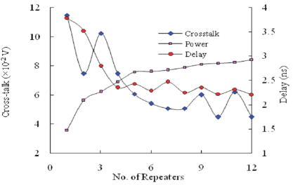
Figure 7. Variation of Line Cross-Talk, Delay and Power with Repeaters for 130nm Technology for Minimum size Repeaters
It is seen from Figures 7 & 8 that cross-talk falls off with increase in number of repeaters. As the number of repeaters are increased, interconnect is divided into smaller subsections. This reduces the effective parasitic capacitance of each subsection and thereby coupling shall also reduce. This is responsible for lesser cross-talk with higher number of repeaters. The effect of repeater insertion on cross-talk is also analyzed for 100nm and 70nm technology nodes for various repeater sizes. These are shown in Figures 9 & 10. Simulation results show that with increase in the size of repeater the cross-talk increases. It is observed that cross-talk reduction is significantly more with the insertion of minimum size repeater.
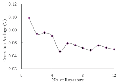
Figure 8. Variation of Cross- Talk Voltages with Number of Repeaters (Size Five Times the Minimum Size)
From Figure 9(a), it is seen that for 100nm technology, cross-talk is minimum for 11 number of minimum size repeaters and is 36.2mV. Cross-talk is 30.9% more for repeaters which are five times in size than minimum size repeaters and 35.6% higher for repeaters which are ten times larger. Figure 10(a) shows that for 70nm technology the cross-talk is 29.3mV for 7 numbers of minimum size repeaters and 63% more if the size of inserted repeaters is made five times higher compared to minimum size. To highlight the variation trend of cross-talk with repeater size the best fit curves are considered.
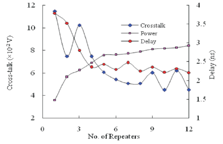
Figure 9(a). Variation of Cross-Talk Voltages with Number of Repeaters
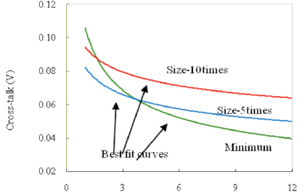
Figure 9(b). Best fit Curves for Variation of Crosstalk with Number of Repeaters for 100nm Technology for three different Repeater Sizes
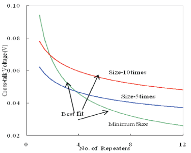
Figure 10(a). Variation of Cross-Talk Voltages with Number of Repeaters
The best fit curves for variation of cross-talk with number of repeaters are shown in Figures 9(b) & 10(b) for 100nm and 70nm technology respectively. These clearly indicate that cross-talk is higher for bigger repeaters. Therefore, increase in size of repeaters has limited scope for cross-talk mitigation in interconnect lines. In the present work minimization of power and cross-talk are the main objectives.
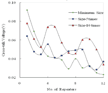
Figure 10(b). Best fit Curves for Variation of Crosstalk for 70nm Technology for Different Size of Repeaters in the Line
Subsequently, for minimization of power and cross-talk the figure of merit considered is the Power Cross-talk Product (PCP). Figure 11 shows the variation of PCP with number of repeaters. It is seen from Figure 11 that for the smallest sized repeaters PCP is minimum, particularly for repeaters more than four. Hence it is proposed that for low cross-talk and low power VLSI design PCP is a useful criterion, along with PDP.
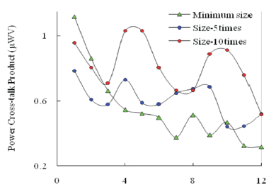
Figure 11. Variation of Power Cross-Talk Product with Number of Repeaters for 70nm Technology
Cross-talk between a pair of interconnect is analyzed in this paper. First dependence of cross-talk on signal transition time and interconnect length are examined with previously reported results in view. The analysis shows that repeater insertion decreases cross-talk in general. However, cross-talk voltage increases with increase in repeater size. Thus smallest size repeaters with a good number of them can yield a reasonably low cross-talk voltage. The results are verified for 130nm, 100nm and 70nm technology nodes using SPICE simulation.