[1]
This paper proposes the design of logic gates for ultra low power applications. The logic gate has been designed in 18 nm technology. In this paper Carbon Nanotube Field Effect Transistors (CNTFET) are introduced for designing the digital circuits. This paper presents the performance analysis of Carbon Nanotube Field Effect Transistor (CNTFET), structure, types of the new nano device, operation, and various gate circuit design using CNTFET. Results of the proposed design are compared with CMOS based gates. All the simulations are done in HSPICE.
A logic gate is a circuit which is used to implement a Boolean function, that is, it performs a logical operation on one or more logic inputs and produces a single logic output. In many applications power of the digital circuit is crucial when it is used in the ultra low power applications, the power consumption of circuit depends on the gates used for the design. Hence designing of gate circuits with low power consumptions are highly desirable. As per the Moore's law number of transistors fabricated on an IC is approximately doubled for every two years. Hence to sustain any IC as per Moore's law, Semiconductor industries are reducing the size of the MOSFET device to increase the number of transistor in integrated circuits. The capabilities of many digital electronic devices are strongly linked to Moore's law interms of processing speed, memory capacity and size of pixels in digital cameras [1]- [5].
When the physical gate length is reduced to below 90nm, many device level creates the increased short-channel effects, reduced gate control, exponentially rising leakage current, severe process variations and unmanageable power densities, which effects substantially the current – voltage characteristic of traditional MOSFETs [2]. To meet the challenges of nano scale CMOS, new circuit techniques together with alternative technologies are used to replace conventional silicon and the current MOSFET-based technology. The scaling of MOSFET has progressed rapidly, it may come to an end soon because of the increased short channel effects and power-dissipation constraints. In order to overcome these problems research groups started to explore new devices to replace the CMOS technology. Many new devices have been reported such as single-electron tunneling (SET), rapid single-flux quantum logic, quantum cellular automata (QCA) and carbon nanotube field effect transistor(CNTFET) [6]-[8].
The Carbon Nanotube Field Effect Transistor (CNTFET) is one of the most promising device among emerging technologies. Carbon nanotube field effect transistor (CNTFET) are currently considered one of the main building block for the replacement of MOSFET based CMOS technology due to their working principles and device structure similar to CMOS. The core of a CNTFET is carbon nanotube. CNTs are the hollow cylinders. Figure.1 shows the structure of graphene sheet and single walled carbon nanotube (SWCNT). Carbon nanotubes are formed, when a graphene sheet of a certain size is wrapped in a certain direction. It may be either single walled or multi-walled. Two atoms in the graphene sheet are chosen, one of which servers the role as origin. The sheet is rolled until the two atoms coincide. The vector pointing from the first atom towards the other is called the chiral vector and its length is equal to the circumference of the nanotube. Depending on their chiral vector, carbon nanotubes with a small diameter are either semiconducting or metallic in nature [9]-[14].
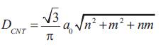
Depending on the angle of the atom arrangement along the tube, the SWCNT can act as either a conductor or a semiconductor,. This is referred to as the chirality vector and is represented by the integer pair (n, m). The diameter of the CNT can be calculated based on the following equation [15],,
where a0 = 0.142 is the inter-atomic distance between each carbon atom and its neighbor. Similar to the MOSFET device, the CNTFET has also four terminals. The currentvoltage (I-V) characteristics of the CNTFET are similar to MOSFET's. The threshold voltage is defined as the voltage required to turn on transistor. The threshold voltage of the intrinsic CNT channel can be approximated to the first order, as the half band gap is an inverse function of the diameter and the equation for threshold voltage is given below [16]-[23].
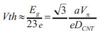
where a = 2.49 Å is the carbon to carbon atom distance, V = 3.033 eV is the carbon π-π bond energy in the tight π bonding model, e is the unit electron charge, and DCNT is the CNT diameter. As DCNT of a (19, 0) CNT is 1.487 nm, the CNT threshold voltage of a CNTFET using (19, 0) CNTs as channels, is 0.293V, The device channel consists of a (19,0), zigzag CNT with a band gap of 0.53 eV and a diameter of 1.5 nm. Figure 2 shows the cross section of a conventional Carbon nanotube field effect transistor (CCNTFET). The gate dielectric is a 4 nm thick HfO2 (k = 16) and the device has channel length of 18nm.
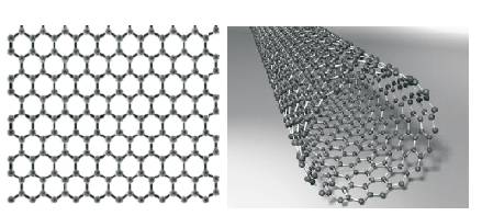
Figure 1. Structure of Graphene and SWCNT
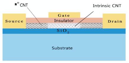
Figure 2. Schematic Diagram of a Carbon Nanotube Transistor
Figure 3. shows the drain characteristics of carbon nanotube field effect transistor with the channel length of 18 nm. Drain voltage is varied from 0 to 0.9v for each constant value of Vgs. Current conduction of CNTFET is high due to high gate capacitance. In CNTFET higk – k material is used as gate dielectric material (k = 16 for proposed design) which provides the high gate capacitance. Figure 3. also shows the characteristics of MOSFET with channel length of 180nm.
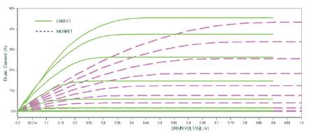
Figure 3. Drain Characteristics of CNTFET and MOSFET
Figure 4. shows the design of NAND gate using CNTFET. This design is simulated using HSPICE with the supply voltage of 0.9v. It uses both P-CNTFET and N-CNTFET. In general for Si CMOS, a PMOS/NMOS ratio of 2 or 3 is used because the NMOS mobility is about 2 or 3 times higher than for the PMOS transistor. However for CNFETs, a PCNFET /NCNFET ratio of 1 is used because the NCNFET and PCNFET have the same current driving capabilities with same transistor geometry. Similarly Figures 5 & 6 show the design of NOR and EX-OR gate using CNTFET respectively.
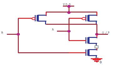
Figure 4. CNTFET based NAND gate
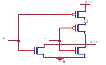
Figure 5. CNTFET based NOR gate
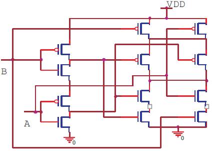
Figure 6. CNTFET based EX - OR gate Circuit
Figure 7 shows the simulated output of NOR gate. Its output is given by the Boolean expression  . Table 1 shows the parameters of the NOR gate. Average power of the CNTFET based NOR gate is 22.2nW where as for MOSFET based gate is 23.8μW. Delay of CNTFET based gate is 49.8ps. Figure 8. shows the results of NAND gate. Output follows the
  function. Table 2 shows the parameters of the gate. Average power consumption of CNTFET based design is 15.7 nW and for CMOS based design 3.9μW. Figure 9. shows the simulated results of EXOR gate. Table 3 shows the parameters of the EX-OR gate.
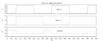
Figure 7. Simulation Results for CNTFET based NOR gate
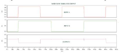
Figure 8. Simulation Results for CNTFET based NAND gate
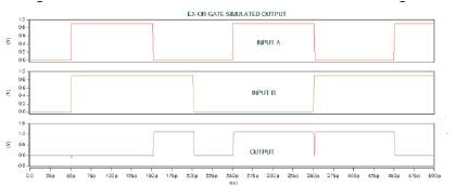
Figure 9. Simulation Results for CNTFET based EX-OR gate
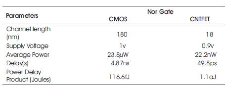
Table 1. Simulated Parameters of NOR gate
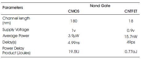
Table 2. Simulated Parameters of NAND gate
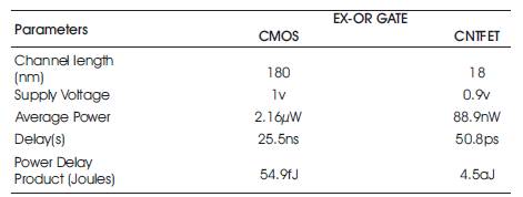
Table 3. Simulated Parameters of EX-OR gate
This paper proposes the new design of logic gates in the 18nm technological node, and design also proposes the CNTFET for ultra low power logic gate design. The performance of the CNTFET based gates increases interms of power consumption, delay, and power delay product when compared to the conventional CMOS based gates.