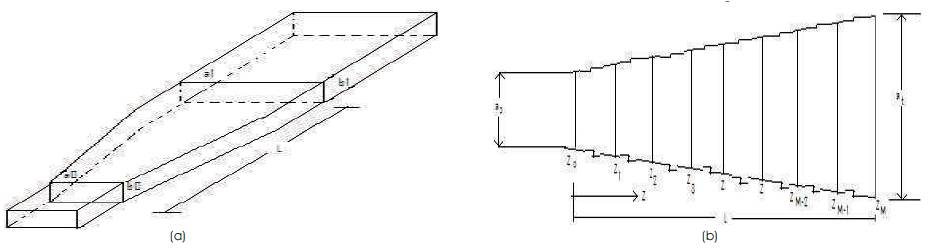
Figures 1(a) & (b). A taper waveguide structure has been divided into small steps
This paper study the thin taper optical waveguide structure by using the step discontinuity model. The technique presented is unique and not being discussed elsewhere. The authors also study the power loss due to step discontinuity effect for the case of an asymmetric single mode planar slab taper waveguide structure. The only assumption, they consider is that there are no reflection of fields at the step discontinuity point. In this paper they also assume that there are no mode conversions due to discontinuity effect and the structure maintain the single mode operation even at the step discontinuity point. The authors deliberately considered the thin taper structure to be valid on single mode operation. The technique presented can be easily extended to more complicated waveguide structure like ridge waveguide structure.
During the last two decades extensive study on analytical/numerical method in the field of optical waveguide has been done by different researchers. Optical waveguides are the building blocks of photonics circuits. They are used as, couplers, switches, splitters, multiplexer and de-multiplexer for optical signals. Although the operation of waveguide devices is well known but their study on the performance characteristics which depends on many parameters like geometry, wavelength and initial field distribution, material data etc are still have a lot of scope to improve. These parameters must be optimized before fabricating a device. Optical fiber communication system requires the WDM optical network components. These components are often called non-uniform planar waveguide structure. In literature there would not found any straight forward analytical technique to analyze these components [1- 10]. One of such taper waveguide structure is shown in Figure 1 (a). This non-uniform waveguide structure or taper structure is divided into small steps discontinuity as shown in Figure 1(b). In next section the researchers will start by analyzing one such step discontinuity between m and m+1 steps. There is no mode conversion due to step discontinuity as such. The waveguide is designed to perform optimally for the fundamental mode only.
In this section the authors will analyze the power loss due to step discontinuity in an asymmetric planar slab taper waveguide structure. The dimension of structure is assumed to be small enough even at the point of discontinuity to be valid on single mode operation hence there is no chance of mode conversion. The analysis somewhat more involve in this case. One of such asymmetric waveguide structure with discontinuity is shown in Figure 2.
Figures 1(a) & (b). A taper waveguide structure has been divided into small steps
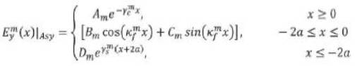
Here the nf represents the film refractive index, ns substrate refractive index and nc cover refractive index. The three indices are chosen such that nf > ns > nc and the guiding layers have a thickness 2a and 4a respectively in mth and m+ 1th section. In the mth region the wave solution is given by [2],
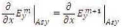
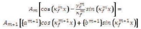
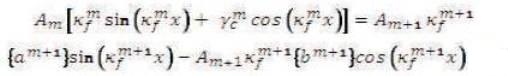
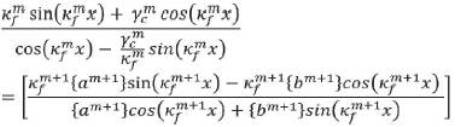
After applying the continuity conditions at various interface we get
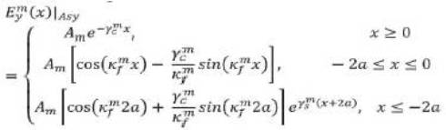
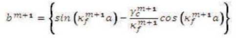
where Am is the amplitude at the x = 0 interface and we get the following eigenvalue equation as
Similarly in the (m+1 )th region the field solution is given by
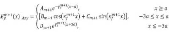
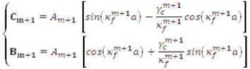
continuity condition at x = a gives
Similarly continuity condition at x = -3a gives
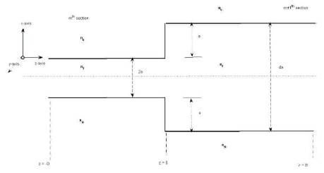
Figure 2. Step Discontinuity in Asymmetric Planar Slab Waveguide
after recombining of all these constants, we get
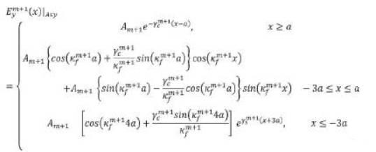
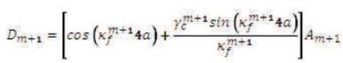
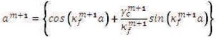
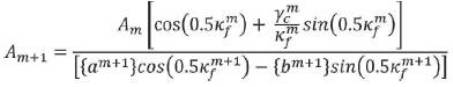
where Am+1 is the amplitude at the x = 0 interface and after boundary condition
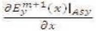
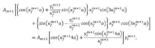
This can be further simplified to get
dividing by  both sides to get
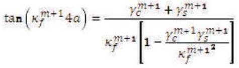
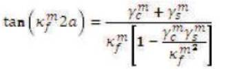
That is a transcendental equation derived for the (m+1)th section having width of the film region 4a that must be solved numerically or graphically. In above equations (1) and (4) they assume that there are no reflections of the fields at the step discontinuity point. These two equations (3) and (10) can be simultaneously solved to get the exact values of Km and Km+1 . Consider the case when nf= 1.49, ns= 1.485, nc= 1.45, a = 0.125 µm and operating wavelength The taper will support only one fundamental mode as shown in Figure 3. The values of βm are found 11.624µm-1 and 11.647µm-1 respectively; hence βm≈βm+1[11-14].
Now if they consider the case when a = 0.75µm and other parameters remain same. Then taper will support multi modes as shown in Figure 4. Comparison of Figures 3 and 4 shows that a = 0.125µm give the single mode operation over a desired wavelength range[15].
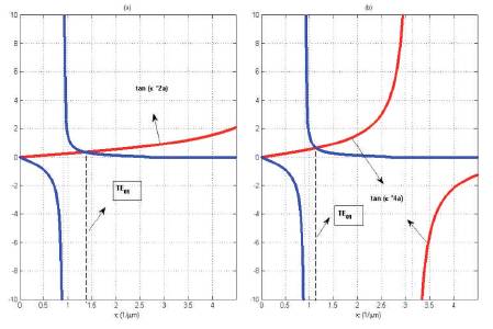
Figure 3. For Extremely Thin Asymmetric Taper Sections There is Only One Allowed Mode, Which Occurs at a) Kfm = 1.3496 µm-1 b) Kfm+1 = 1.1409 µm-1
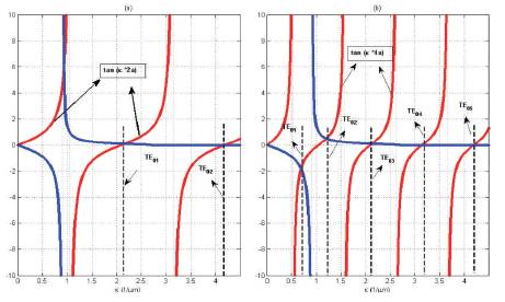
Figure 4. The Graphical Solution to the Eigenvalue Equation for a Multimode Asymmetric Waveguide Structure
By applying the similar procedure as for symmetric waveguide structure the continuity condition at
and
 at z=0
leads the following two equations [1]
where
and
are the constants. Equations (11) and (12) can be simultaneously solved to get
This equation is required for the graphical solution to know the optimum value of x for which eq. (13) will satisfy. The result is shown in Figure 5. It is apparent that maximum power will coupled from taper mth section into m+1th section only x≈-0.5µm Finally this condition will lead m [16-18],
where Kfm and Kfm+1are measured in µm. By using condition (14) and after applying the continuity condition at step discontinuity point, we will get the following optimum equation
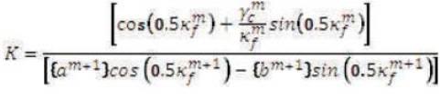
Here K is constant which can be easily evaluated and is given by,
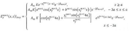
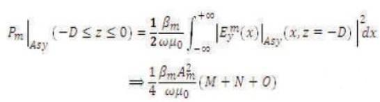
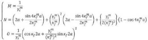
The unknown constant Am can be found by normalizing the input power to unit one which associated with the mode (per unit length in the y-direction) given by [20-24],
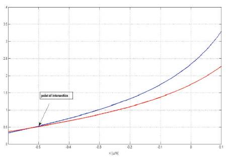
Figure 5. Optimum Power Coupling at Step Discontinuity Will Take Place Only if x ≈ -0.5µm (λ= 0.8µm)
where
This power will remain constant till z = 0 point.
Power carried by fundamental TE01 mode of mth and (m+1)th isolated sections is shown in Figure 6. Figure 7, shows the variation of constants Am and Am+1 (PTotal = 1) with wavelength. The fractional power carried by the film region of the mthsection of asymmetric waveguide can be found by the expression
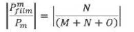
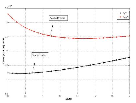
Figure 6. Power carried by mth and ([m+1)]th Isolated Sections
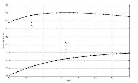
Figure 7. Calculated Normalized Constants Am and Am-1 (PTotal = 1)
Figure 8. The Fractional Power (%) carried by the films of mth and ([m+1)]th Isolated Sections
The fractional power (%) carried by films region of mth and ([m+1)]th sections is shown in Figure 8. It shows that at lower wavelength the power confinement is large which saturates rapidly at higher wavelength region.
Now consider the taper discontinuity at z = 0. Then the power carried by (m+1)th section of the taper can be described by
where
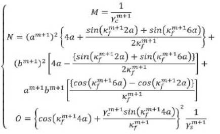
Figure 9 shows the effect of step discontinuity on power carried by mth and (m+1)th section. It reveals that there is substantial power loss due to discontinuity.
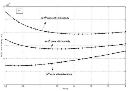
Figure 9. The Effect of Step Discontinuity on Power Carried by mth and ([m+1)]th Sections
Finally the power loss (%) due to discontinuity at z = 0 is given by

Figure 10 shows the power loss due to step discontinuity for various values of position x.
Figure 10. The Power Loss (%) Due to Step Discontinuity for Various Values of Position x (µm)
In this paper the authors have studied the effect of step discontinuity on single mode asymmetric planar slab taper waveguide structure. We found that the power loss due to step discontinuity is substantial. The results are found to be an accurate enough. The interpretations of the results are done at the end of the paper. By adopting the few assumptions the results have been derived. For more rigorous analysis of step discontinuity affect one need to consider the back reflection of the fields and mode conversion affect at the step discontinuity point. The technique presented in this paper is general can be easily extended to more complicated structure.