(1)
This paper presents the simulation analysis of a 2.4 GHz Quadrature Voltage Controlled Oscillator (QVCO), for low-power, low-voltage applications. Cross coupled LC VCO (Inductor-Capacitor Voltage Controlled Oscillator) topology is utilized to realize QVCO. With the passive coupling achieved from the MOS transistors, power consumption is minimized while maintaining a small chip area. The variable capacitors and the inductors are designed using ANSYS and imported through DAC components in ADS (Advanced Design software). Accurate simulation of the QVCO is performed in the software environments and the results are provided. This QVCO provides quadrature signals at 2.4 GHz, achieves a peak to peak voltage of 0.65 volts with a simulated low power consumption of 5.8 mA from a power supply voltage of 0.6 volts. The simulated QVCO produces frequency tuning from 2.1 GHz to 2.60 GHz (20.83%) with a control voltage varying from 0-0.3 volts. The output power level of the QVCO is -7 dBm, with an improved predicted quality factor of 60 and a phase noise of -134 dBc/Hz, 1MHz far from the carrier frequency.
The fast growing market in wireless communications has led to the need for low-power, low-noise voltage controlled oscillators. Especially for mobile wireless communications, low power operations are of very importance as the battery lifetime depends on the power consumption. Quadrature signals can be generated by feeding the differential outputs of the VCO to a poly phase filter (Steyaert and etal., 2000; Behbahani and etal., 2001) , letting the VCO work at double the desired frequency and pass through frequency division (Ravi and etal., 2002; Maligeorgos and etal., 2000), and coupling identical LC VCO circuits ( Ham and Hajimiri 2001; Tiebout 2001) to each other. The poly phase filter approach introduces substantial power consumption due to the attenuation by the resistance and the capacitance in the circuit. The frequency dividing approach avoids the pushing/pulling effect on the VCO, however, the existence of frequency divider and high frequency VCO result in increased power consumption.
A more attractive approach to direct quadrature synthesis relies on the possibility of effective coupling of two identical LC VCO circuits. The first coupling approach is the best known parallel coupling ( Rofougaran and etal., 1996 ), where coupling between the two VCOs is enforced by transistors. While this coupling delivers low power, low amplitude and phase errors, it produces high phase noise. Introducing a phase shifter as reported in ( Van der Ven and etal., 2001 ) offers better phase noise per formance, however it increases the power consumption. Several other coupling techniques have been reported like back gate coupling (Kim and etal., 2004), super-harmonic coupling ( Gierkink and etal., 2003 ), and transformer coupling ( Ravi and etal., 2003). In addition to this current reused QVCOs are also proposed ( Nam-Jin Oh and etal., 2005). However these approaches have their own merits and demerits, the urge of low power design of QVCO while maintaining low phase and amplitude errors still exists. In this work an attempt is made to make use of the VCO, reported ( Sreeja and Radha 2011), to design a low power QVCO.
The QVCO is designed to oscillate at 2.4 GHz, and to determine the impact on the performance parameters. Figure 3(a) shows the LC VCO employed in this work. LC VCO provides outstanding phase noise and jitter performance at high frequencies compared to other topologies. Cross coupled pair LC VCO topology is selected for this design due to its high output voltage swing, balanced differential output and symmetrical structure. From the well known theory of oscillators, the positive feedback transistors M3 and M4 are used to achieve negative input resistance, with which positive resistance of LC resonant circuit might be eliminated bringing on zero-dampen oscillating property. PMOS transistors M1 and M2 are used to generate the required bias current. However, this topology provides the above merits, it contains an inductor and a varactor in its tank circuit which are large area components. In order to reduce the die area of the resonant circuit, MWCNT based pulse inductor is integrated with Micro scale varactor. In order to reduce the required supply voltage and to eliminate additional noise contribution, the tail current transistors in a conventional cross-coupled VCO can be replaced by on-chip inductors ( Troedsson and Sjolamd 2002 ).
In this work the tail current transistors are replaced with MWCNT bundle based inductor. For an enhanced voltage swing under an ultra-low supply voltage, the capacitive feedback technique can be employed ( Wang 2001). The capacitive feedback loop is established by C1 and C2 Due to the use of the on-chip inductor and the capacitive feedback loop, the drain and source voltages can swing above the supply voltage and below the ground potential. Consequently, the output swing of the VCO is enhanced, leading to a superior close-in phase noise. Since the feedback capacitors are employed in the source terminals of the cross-coupled transistors, a more effective controlled mechanism of the tank resonance is presented. Therefore, a reasonable frequency tuning range can be achieved even with a reduced voltage range for the controlled signal. The variable capacitors CA, CB and CC represent the Micro scale varactor and CB is modelled as two series capacitances to maintain the , symmetry of the circuit. L1 and L2 are modelled as on-chip inductors. Figure 3(b) shows the circuit diagram of the quadrature LC VCO. Two identical LC VCO circuits together with the coupling structure as shown in Figure 1(a) & (b) are utilized to generate quadrature phase sinusoidal signals. The transistors are biasd at zero dc current and operate as passive elements. Note that the coupling transistor is replaced by parallel RC network in Figure 2. The design parameters of the simulated VCO are listed in Table 1.
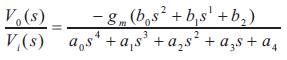
Using laplace transform analysis the approximated transfer function (single ended output to input) can be derived as,
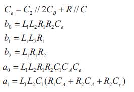
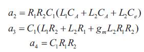
where the coefficients of the numerator and denominator are as follows:
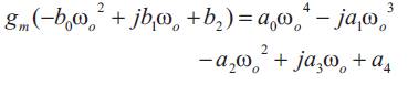
The circuit oscillates if equation (1) is equal to -1, and at the oscillation frequency ω0,
With proper assumptions and simplifications the oscillation frequency can be approximated as
Assuming L1 = L2 = Lp and R1 = R2 = Rp equation (5) and (6) can be simplified as,
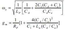
From equation (7) it is seen that the oscillation frequency has two parts, in its theoretical derivation. As conventional LC Voltage Controlled Oscillators,  contributes the major part of the oscillation frequency and the second part
  further enhances the oscillation frequency. However, the fixed capacitance C1 degrades the oscillation frequency compared to, ω0 could be still improved by the numerator part 2(CA +Ce). From equation (7) it is noticed that the fixed capacitance C1 increases (since < 1) the trans-conductance which helps us to initiate successful oscillations. Therefore, a design trade off is established between the tuning range and the trans-conductance based on C1 . Moreover, gm should be maintained to a value with which oscillations can occur. However a reasonable tuning range can be obtained using the four plate Micro scale varactor. It can be concluded that by selecting suitable and optimal values for the capacitors better theoretical performance can be seen from the designed oscillator.
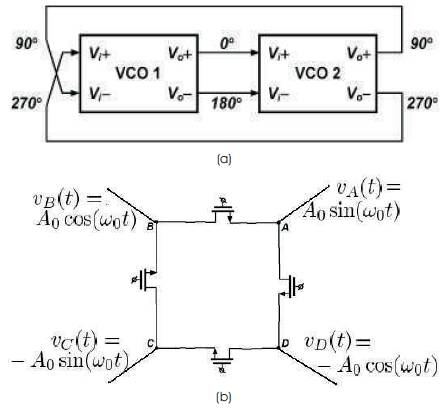
Figure 1(a). Schematic of the coupling Structure of QVCO (b) Equivalent circuit model of the coupling structure
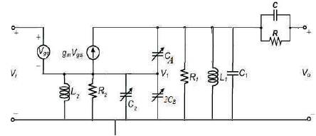
Figure 2. Simplified half circuit model of the proposed VCO
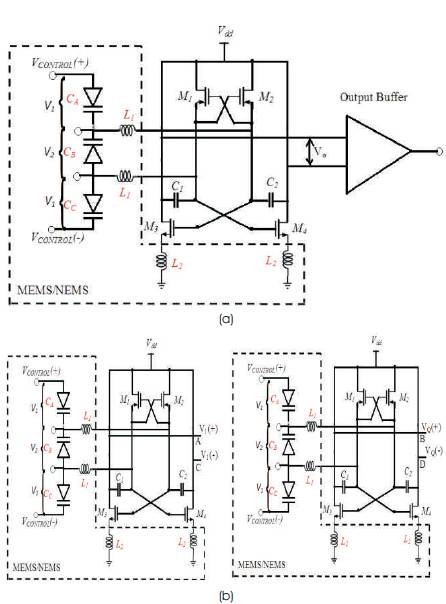
Figure 3. (a) Schematic of the proposed LC CMOS VCO showing the replacement of tail current transistors and the feedback gate capacitance (b) QVCO structure
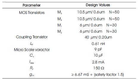
Table 1. Design Parameters
Layout of the proposed QVCO is designed using a 90nm CMOS process in Microwind environment. The CMOS section of the QVCO structure is symmetrical. The active layout area of the QVCO is 710um x 760um, including the bonding pads. The distance between the components is minimized in order to reduce the phase noise, and the layout is made as symmetrical and compact as possible to ensure differential operation and reduce parasitic inductance or capacitance.
The time referenced oscillation shown in Figure 5 is generated in ADS environment using the QVCO topology. The oscillation frequency is measured as 2.40 GHz, with the variable capacitor tuning voltage v1 (actuation voltage of the capacitor) at 0.072 volts, and v2 (actuation voltage of the capacitor) at 0.9 volts. All simulations are performed with 0.6 volts power supply voltage and a current consumption of 5.8 mA in the core circuit.
The simulation results of phase noise using HB method with ADS is shown in Figure 6. Since the proposed QVCO is operated under ultra low dc voltage, the cross coupled transistors are potentially biased in the weak inversion region. The phase noise is simulated as -134 dBc/Hz at an offset frequency of 1 MHz from the carrier frequency. It is noted that, for low power operations the cross coupled transistors may contribute more noise to the LC tank as the supply voltage decreases. Hence, it imposes a fundamental limitation on the phase noise of the QVCO for ultra low power and low voltage application.
The tested circuit is tranferred to the layout for further simulation. Layout of the QVCO is simulated, and the simulation results are shown from Figures 7-9. Figure 7 shows the simulation results when v is varied from 0-0.3 v and v2 is kept at 0.9 v. When the control voltage is increased above Vdd /2 (0.3 v) the device stops oscillating, and a dc voltage of 0.6 volts is produced as output voltage. Thus the maximum level of the control voltage is Vdd /2. Figures 8 and 9 shows the current waveforms of PMOS and NMOS transistors respectively. The transistors are sized to achieve the design specifications. The power consumption of the device with a supply voltage of 0.6 volts is approximately 5.8 mW. The device is simulated with a power supply voltage of 1.2 volts and the current consumption is found to be 11.9 mA. Also during the simulations it was noted that the phase noise has an inverse relation with the supply voltage. The phase noise may be improved at higher supply voltages.
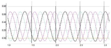
Figure 5. Output oscillations of QVCO circuit simulated using ADS
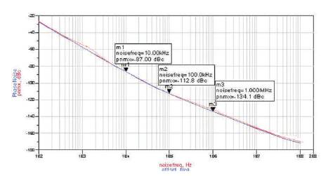
Figure 6. ADS Simulated phase noise as functions of offset and noise frequency
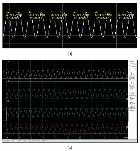
Figure 7. (a) Simulated frequency zoom view (b) Output oscillations of QVCO layout simulated using Microwind-Control voltage v1 varies from 0 volts to 0.29 volts and v2 is kept at 0.9 volts
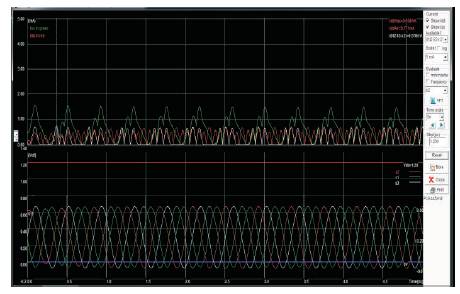
Figure 8. Output voltage and current waveforms (PMOS) of QVCO layout simulatedusing Microwind-Control voltage varies from 0 Volts to 0.3 Volts
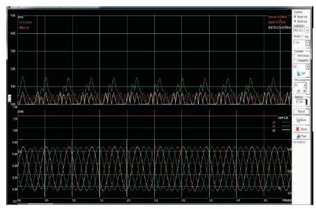
Figure 9. Output voltage and current waveforms (NMOS) of QVCO layout simulated using Microwind-Control voltage varies from 0 Volts to 0.29 Volts
Table 2 shows the performance characteristics and the design variables of the QVCO. As in the table, the designed QVCO exibits a tuning frequency range of 500 MHz, with 2.4 GHz as center frequency which leads a tuning percentage of 20.83. Because of the trade-off between the phase noise and the tuning frequency range, that the phase noise of the oscillator is inversely proportional to the tuning frequency range, the tuning frequency range is limited. The tank circuit impedance exhibits an inversely proportional relationship with the oscillation frequency.
When the tank circuit impedance is lowered, the start-up gain is reduced as well as output voltage swing. Hence the value of the tank circuit impedance is carefully chosen to avoid these issues. The quality factor of the resonant circuit at 2.4 GHz is calculated as 69, which provides a quality factor of 63 for the QVCO at the same frequency. With the additional circuitry included, the quality factor of the QVCO has been predicted as 60 at 2.4 Ghz. The gate-source and the drain source capacitance of the PMOS and NMOS transistors are measured between 0 to 3.5 fF.
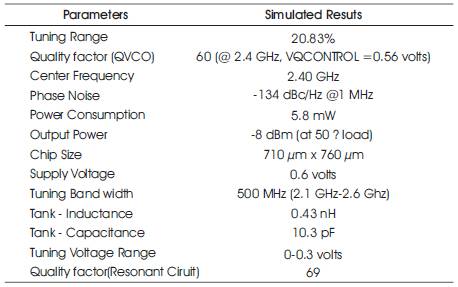
Table 2. Simulated results of QVCO
A 2.4 GHz QVCO is simulated and the results of the simulation are analysed. The results indicate QVCO operation at a center frequency of 2.4 GHz with a quality factor of 60. The chip size is 710 μm x 760 μm. The simulation predicts phase noise of -134 dBc/Hz at a power supply voltage of 0.6 V. The simulated oscillation amplitude is maintained slightly above Vdd using the feedback capacitors. The simulation operational conditions indicate that the device consumes ultra low power at 5.8 mW, including the buffer. Further the fabrication of the QVCO is expected.