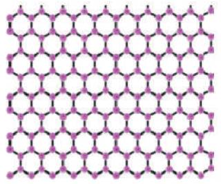
Figure 1. Structure of Graphene
Carbon Nanotube Field Effect Transistors (CNTFET) are new nano-scaled devices for the digital circuits. In MOSFET based digital circuits when the channel length is much smaller than a micrometre is a challenge, and creates the problems in device fabrication, which limits advancing the integrated circuit. Small size of the MOSFET, below a few tens of nanometres creates the low Trans-conductance, gate oxide leakage, low ON-current, Mobility degradation and increased delay. Problems observed in the MOSFET, when size is reduced are avoided in CNTFET, since in case of CNTFET, carbon nanotube is used as channel and high-k material is used as gate dielectric. In this paper, the authors present the simulation results of semi-conducting Carbon Nanotube Field Effect Transistors based logic gates using HSPICE.
Semiconductor industries are reducing the size of the MOSFET device to increase the number of transistor of an integrated circuits to sustain any IC as per Moore's law. According to Moore's law number of transistors placed on an IC doubles approximately every two years. The capabilities of many digital electronic devices are strongly linked to Moore's law interms of processing speed, memory capacity and size of pixels in digital cameras [1]. When the physical gate length is reduced to below 65 nm, many device level creates the increased shortchannel effects, reduced gate control, exponentially rising leakage currents, severe process variations and unmanageable power densities, which effects substantially the current – voltage characteristic of traditional MOSFETs[2]. To meet the challenges of nano scale CMOS, new circuit techniques together with alternative technologies is used to replace conventional silicon and the current MOSFET-based technology. Recently, there have been tremendous advances in carbon nanotube (CNT) technology for nano-electronics applications. The Carbon Nanotube Field Effect Transistor (CNFET) is one of the most promising device among emerging technologies. The CNFET offers many potential advantages with respect to silicon-based technology. Its operation principles and device structure are similar to CMOS, and therefore the mature design infrastructure of this latter technology can be utilized, together with its fabrication process [3].
Carbon nanotubes (CNTs) are currently considered as promising building blocks of a future nano electronic technology. CNTs are hollow cylinders composed of one or more concentric layers of carbon atoms in a honeycomb lattice arrangement as shown in Figure (1). This results in a structure with a very high aspect ratio and 1D behavior. CNTs are classified as either single-wall (SWCNT) or multi-wall (MWCNT), depending on the number of layers of material forming the walls of the cylinder. Structure and properties of the layers are common to both types of tubes. Single-walled nanotubes (SWCNTs) typically have a diameter of 1–2 nm and a length up to several micrometers is shown in Figure 2 [4].
Graphene is used as a starting point for the development of a model of the inter-related physical and electronic properties of CNTs. The physical structure of a CNT is described in terms of a sheet of graphene rolled up along a chiral vector, which indicates the orientation of the carbon lattice relative to the axis of the tube. The orientation of the carbon lattice is critical in determining the electronic properties of the CNT. This is one of the most significant properties of CNTs and is unique to solid state physics. In addition, depending on the detailed arrangement of the carbon atoms the SWCNTs can be metallic or semiconducting [5].
Figure 1. Structure of Graphene
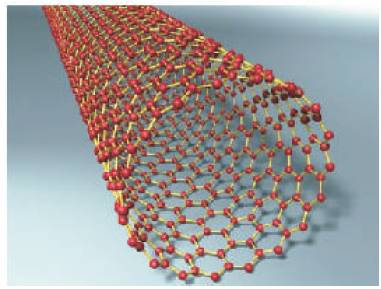
Figure 2. Single Walled Carbon Nanotube
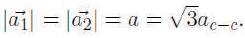
Graphene is a two-dimensional (2D) hexagonal lattice of covalently bonded carbon atoms. Each atom is bonded to three adjacent atoms in the same plane. Figure 3 shows the schematic of the graphene lattice including the lattice vectors, a1 and a2 , that define the lattice geometry[5][6]
The lattice vectors are defined in terms of the lattice constant, a, which is a geometric function of the carboncarbon bond distance, ac-c (0.142 nm). Excellent carrier transport properties of single-wall carbon nanotubes (CNTs) lead to a strong interest in potential applications of CNTFETs in digital and radio-frequency (RF) electronics.
Figure 3. Chiral Vector
CNTs properties are strongly dependent on their chirality and diameter. The chirality is related to the degree of the twist of the lattice of the tube and can be described by the chiral vector. The chiral vector is a circular vector that is perpendicular to the axis of the tube. It is a linear combination of the base vectors a1 and a2. In mathematical terms the chiral vector is defined as [5]-[8]
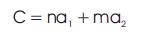
where n and m are integers. Graphical representation of the chiral vector is shown in Figure 3.
This paper presents the simulation of carbon nanotube field effect transistor based logic gates. The diameter of the CNT can be calculated using the following equation [9]

Where a0 = 0.142 is the inter-atomic distance between each carbon atom and its neighbor. Similar to the MOSFET device, the CNTFET has also four terminals. The currentvoltage (I-V) characteristics of the CNTFET are similar to MOSFET's. The threshold voltage is defined as the voltage required to turn on transistor. The threshold voltage of the intrinsic CNT channel can be approximated to the first order, as the half band gap is an inverse function of the diameter and the equation for threshold voltage is given below[10][11].
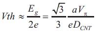
Where a = 2.49 Å is the carbon to carbon atom distance, Vπ = 3.033 eV is the carbon π-π bond energy in the tight bonding model, e is the unit electron charge, and DCNT is the CNT diameter. As DCNT of a (19, 0) CNT is 1.487 nm, the threshold voltage of a CNTFET using (19, 0) CNTs as channels, is 0.293V, The device channel consists of a (19, 0), zigzag CNT with a band gap of 0.53 eV. Figure 4 shows the cross section of a conventional Carbon nanotube field effect transistor (C-CNTFET).
The gate dielectric is a 2 nm thick HfO2 (k = 16) and the device has channel length of 100nm. We compute the intrinsic delay of the device at the ballistic limit. The recent progress on quasi one-dimensional nanowire contacts and on the CNT array channel, however, may significantly reduce the parasitic capacitance and eventually lead to a performance close to the intrinsic limit. [12]-[14], Figure 5 shows drain current as a function of gate voltage and when drain voltage is 1V,
The inverter is the fundamental logic gate for digital circuit design. Many of the basic principles employed in the design and analysis of an inverter can also be applied to complex logic circuits such as NOR, NAND, XOR, and FULL ADDER. To compare the performance of the MOSFET and CNFET, the P-Transistor/– Transistor ratio of the MOSFET and CNFET inverters should be established. In general for Si CMOS, a PMOS/NMOS ratio of 2 or 3 is used because the NMOS mobility is about 2 or 3 times higher than for the PMOS transistor. However for CNFETs, a PCNFET /NCNFET ratio of 1 is used because the NCNFET and PCNFET have the same current driving capabilities with same transistor geometry [3]. In CMOS design, the width of the MOSFET is adjusted to change the PMOS/NMOS ratio. However in a CNFET, the number of tubes is the design parameter (such as the W/L ratio in conventional design) for changing the current and resistance Figure (6), (7), (8) shows the design of CNTFET based NOT, AND, OR logic gates respectively.

Figure 4. Schematic Diagram of a Carbon Nanotube Transistor
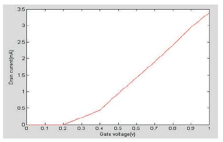
Figure 5. Drain Current IDS for VDS = 1V

Figure 6. CNTFET based NOT gate Circuit
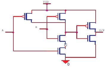
Figure 7. CNTFET based AND gate Circuit

Figure 9 shows the numerical results of intrinsic delay versus channel length of the CNTFET,
In this paper simulation of CNTFET based digital circuit is presented. Simulation is done using HSPICE, for the simulation initially library file model has been created same as MOSFET library file creation. In this simulation CNT length is 100nm, diameter of the CNT is 1.5nm. oxide thickness is 2nm, dielectric constant k=16. Both PCNTFET and NCNTFET model library file is created. Complementary logic is used to simulate the CNTFET based gates.
Performance of CNTFET in current conduction is high due to their high gate capacitance; this high capacitance value increase ON state current of the device, Gate capacitance value is increased by using high-k dielectric material as gate dielectric. Figure 10 shows the output of NOT gate, Figure 11 shows the results of AND gate, Figure 12 shows the performance of OR gate. Since CNTFET can be fabricated in the small chip area, this device will be the best replacement for the MOSFET based digital circuit.
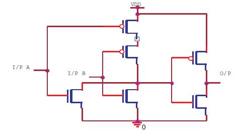
Figure 8. CNTFET Based OR Gate Circuit
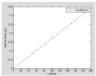
Figure 9. Numerical results of Intrinsic delay versus the channel length
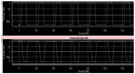
Figure 10. Simulation Results for CNTFET Based NOT Gate
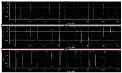
Figure 11. Simulation results for CNTFET based AND gate
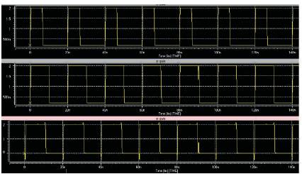
Figure 12. Simulation Results for CNTFET based OR gate
This paper has investigated the application of CNTFETs in NOT, AND, OR gates. As the threshold voltage of the CNTFET can be easily controlled by changing the chirality vector of the CNTs, digital circuit can be designed for the required threshold voltage. The best chirality for the PCNTFETs will give high stability, and low power consumption.