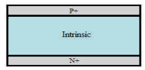
Figure 1. PIN Structure
In this paper, a parametric study of silicon based PIN diode and Silicon Plated Germanium (SPG) PIN diode is performed th and comparative study is presented. SPG is a germanium diode containing 1/10 width of N+ region doped with silicon. The comparative study is performed on different parameters such as P+ layer and N+ layer concentration, Intrinsic layer thickness, P+ region and N+ region width, and Intrinsic region width. The results obtained from simulation shows that the forward current conduction of SPG PIN diode is greater than silicon device and hence, the resistance offered by SPG is far less than silicon device . The whole work of this paper is done with the help of SILVACO simulator tool.
The PIN diode performance ability lies in chip configuration, type of semiconductor materials, and also on different modes of operation of the device (Shuhaimi et al., 2010). The geometrical arrangement of PIN diode incorporates an intrinsic layer in-between two highly concentrated P+ and N+ region. The intrinsic region acts as a charge storage when it is forward biased, as well as it also facilitates large reverse breakdown voltage and a very low level of capacitance (Iturri-Hinojosa et al., 2010). The amount of charges is responsible for the resistivity in intrinsic region (Sze and Ng., 2007). The PIN diode resistance is the result of only forward bias current (Jubadi and Noor, 2010). The PIN diode has tremendous application in power electronics due to its intrinsic layer, as it can also perform at higher voltages (Doherty, 1998). Radio Frequency switching (RF switching) and Radio Frequency attenuators (RF attenuators) are one of the promising applications of PIN diode along with other applications such as photodiode, phase shifters and many more (Aditya et al., 2015). The switching action of PIN diode is accounted by variation of intrinsic region resistance at an appropriate signal level (Leenov, 1964).
As it is known that the Germanium PIN diode has very high current rating and low voltage drop, certain PIN diodes cannot withstand this much of current. For Silicon PIN diode, although the voltage drop is little higher, the current obtained is very low. Here, the proposed device has current rating in a range suitable for PIN diodes, and a voltage drop little higher than germanium. The current range obtained here is much better than silicon diodes, hence the resistance offered in forward bias is also very less as compared to silicon diode. Hence, the proposed device has its characteristics in between silicon and germanium. The general PIN diode structure is depicted in Figure 1.
Figure 1. PIN Structure
For a device designer, current conduction is always a matter of choice; so here two devices have been analyzed for better device performance in terms of current conduction, and thus providing improvement for the silicon device.
The simulation work is performed on SILVACO-ATLAS Software Tool (Silvaco International, 2015). This paper presents two PIN devices based on different materials. The forward characteristics of these devices are analyzed and the consequences of different device parameters on the device performance are determined. The two devices are: (1) Silicon diode and (2) Silicon Plated Germanium diode which is a germanium diode containing 1/10 width of N+ region doped with silicon, and abbreviated as “SPG”. The device specification 21 chosen are the same for both devices which contain 10 -3 cm doping concentration for both P+ and N+ region 14 -3 and about 10 cm doping for intrinsic region. The P+ and N+ layers widths are taken as 12 μm, whereas intrinsic layer width is taken as 44 μm. The length of the device is taken as 10 μm. The diagram for SPG is shown in Figure 2.
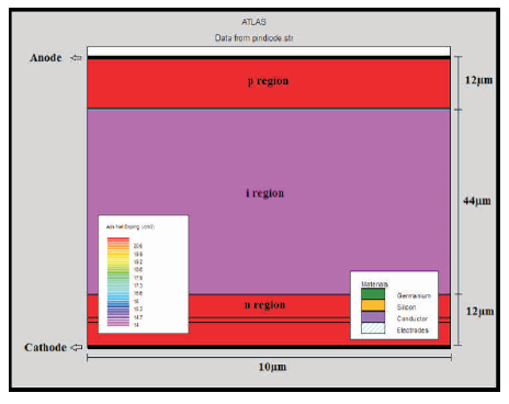
Figure 2. PIN Structure of SPG
The graphs for Silicon and SPG devices are shown in Figures 3 (a) and 3 (b) respectively.
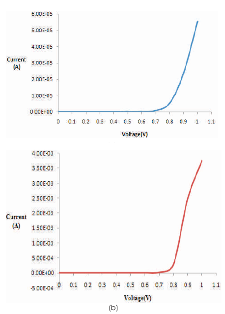
Figure 3. Current vs Voltage Graph for (a) Silicon (b) SPG
From Table 1, it is clear that for silicon device, the current -7 obtained is 8.55 x 10 ampere (A) at the threshold voltage of 0.7 V. Whereas for SPG device, the current obtained is -6 1.77 x 10 A at 0.6 volt which is 2.07 times greater than silicon diode. Hence, it is concluded that, SPG device is far better than Silicon device.
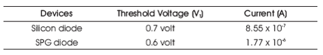
Table 1. Threshold Voltage and Current Value for Silicon and SPG Device
The current versus resistance graph upto 1 Volt for both the devices is shown in Figure 4.
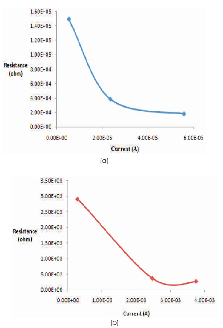
Figure 4. Resistance vs Current Graph up to 1 Volt for (a) Silicon (b) SPG
From Figure 4, it is analysed that the forward resistance offered by SPG is very less as compared to Silicon device. 2 Around 1Volt, the resistance offered by SIG is 2.67x10 Ω while the silicon device offers 1.8x10 Ω resistance.
The analysis of the consequences of various device parameters on the I-V characteristics of both the devices are detailed below.
In this structure, the P+ and N+ region widths are chosen as 12 μm and the intrinsic layer width as 44 μm, while the 14 -3 concentration of intrinsic region as 10 cm . The Current and corresponding resistance values for both Silicon and SPG devices up to 1 Volt are given in Table 2. Table 3 depicts the obtained current value for different P+ and N+ concentration for both the devices. From Table 3, it is clear that for both the devices, the current value increases on increasing the P+ and N+ region impurity concentration.
Table 2. Current and corresponding Resistance Values for both Silicon and SPG Devices up to 1 Volt
Table 3. Current Obtained for Different P+ and N+ Doping Concentrations at 1 Volt
This time, the P+ and N+ concentrations are fixed at 10 -3 cm , whereas the intrinsic concentration is varied. The P+ and N+ region widths are 12 μm and the intrinsic width is 44 μm. Figure 5 shows the current values at 1 Volt for three different concentrations of P and N region for Silicon and SIG.
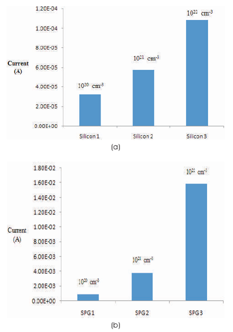
Figure 5. Current Values at 1 Volt for Three Different Concentrations of P and N Region (a) Silicon (b) SIG
From Table 4, it can be concluded that for silicon device the current value decreases on increasing the intrinsic region concentration, while for SPG devices, the current value shows no variation. Here, the concentration chosen must be in a range so that the intrinsic region property should be maintained.
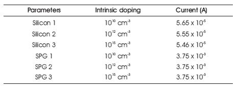
Table 4. Obtained Values of Current for Different Intrinsic Region Doping Concentrations at 1 Volt
Here the P+ and N+ impurities are taken as 10 cm and 14 -3 intrinsic doping is taken as 10 cm . The intrinsic width is taken constant at 44 μm while the P+ and N+ widths are varied.
From Table 5, it is clear that for 6 μm and 12 μm width, the current for both the devices shows no variation, while for 20 μm width, the current for silicon device decreases whereas it remains constant for SPG. Hence, it is clear that choosing SPG device will be a better option since the current does not decrease on increasing the device length, which means the device P and N lengths will not be a restriction for SPG devices.
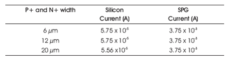
Table 5. For Different P+ and N+ Width the Value of Current is noted at 1 Volt
Now, the intrinsic width variation effect on both the devices are investigated. For this, the device specification 21 -3 14 contains 10 cm impurities in P+ and N+ layers and 10 -3 cm impurities in intrinsic layer. The dimensions of P+ and N+ layers are same as 12 μm. Figure 6 shows the current values at 1 Volt for three different intrinsic widths for Silicon and SPG.
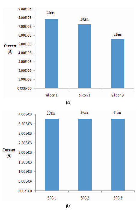
Figure 6. Current Values at 1 Volt for Three Different Intrinsic Widths for (a) Silicon (b) SPG
Table 6 depicts that for silicon, the current decreases on increasing the intrinsic width, while for SPG, the current is independent of intrinsic width. Hence, here is an advantage of using the SPG device, as one can choose any intrinsic width as per device convenience.
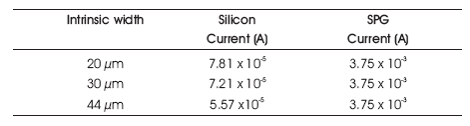
Table 6. Effect of Intrinsic Width on Current Value of Devices for 1 Volt
A new device model, SPG, has been proposed in this paper, and its device characteristics are found to be better than the traditional silicon diode. The forward current conduction is also greater than silicon, hence the resistance offered by SPG is far less than the silicon device. Also, the diode characteristics on four parameters are analyzed which that, on increasing the P and N region concentration, shows the current increases for both the devices. Hence one can choose the appropriate doping based on current values required. The study on intrinsic concentration depicts that, the current decreases for silicon device while it remains constant for SPG devices. As the device designers always opt for a device with better current conduction, the SPG device provides a better alternative for silicon device.