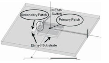
Figure 1. Model of the Proposed Frequency Reconfigurable Radiator
This paper presents design of a microstrip patch antenna with cantilever type Micro-Electro-Mechanical Systems (MEMS) switch to achieve reconfigurability. The primary and secondary radiators are connected by a cantilever MEMS switch. Normally, the MEMS switches are fabricated over high resistive materials whereas planar radiator is designed on low dielectric substrate. Lateral etching based micromachining of Silicon (Si) substrate is proposed in the design to enhance its performance by accommodating a MEMS switch on it. In order to visualize the effect of bandwidth (BW) with respect to the depth of etching, a parametric study was carried out. The simulation results validate the reconfigurability of the design by observing shifts in resonance frequency of 600 MHz by changing the state of MEMS switch.
In recent years, compact size microwave circuits are very promising due to their unprecedented growth in modern communication era. In order to broaden the application area using these circuits, tunable components are getting wide attention in some applications, viz. matching networks, filters. These components are used to design circuits through which the same circuit can be reused for different operations at different frequencies of interest. Microwave switches (e.g. Ferrite, Pin, Field Effect Transistor (FET)) are the most fundamental components. They have versatile applications and can be utilized in various approaches. Among them, Micro-Electro-Mechanical System (MEMS) switches are the most emerging technology. Applications of MEMS switches are very lucrative as MEMS based switches have very low insertion loss, negligible power consumption and smaller volume as compared to its counterpart e.g. PIN, FET switches. Conventionally MEMS switches are fabricated over high resistive Silicon (Si) or Gallium Arsenide (GaAs) substrate to achieve low insertion loss and higher isolation (Haupt and Lanagan, 2013; Karmakar et al., 2013; Papapolymerou et al., 1998).
Microstrip patch antenna configuration is most popularly used in the field of modern communication due to ease of fabrication, light weight, and low fabrication cost even though it has some disadvantages like narrowband, low efficiency. Microwave patch is fabricated over low dielectric constant material, e.g. Duroid (Lucyszyn and Pranonsatit, 2013 Wong, 2004).
Reconfigurability of antenna implies the capacity to change an individual radiators fundamental characteristics through mechanical, electrical or other means (Christodoulou, 2003; Haridas et al., 2008; Peroulis et al., 2005; Topalli et al., 2005). Compact circuit designs is typically achieved in high dielectric constant material but the radiation performance entails in electrically thick low- index materials. The perfect solution is to integrate the patches on electrically thick low-index regions while the circuitry remains on the high-index regions over the same substrate.
In this design, a microstrip patch antenna is integrated with the cantilever type MEMS switches over high resistive Silicon substrate. The Si material is etched from underneath of patch region to create a cavity. Micro-machined patch configuration shows superior performance of higher bandwidth and efficiency over the conventional patch (Papapolymerou et al., 1998). The micro-machined part of Si produces low dielectric constant and is suitable for radiative application. The design has two patches connected through electro-statically actuated cantilever MEMS switch. For the feed of patch, conventional inset feed is used (Balanis, 1997; Pan et al., 2005; Wong, 2004). The main patch is designed for the resonance frequency of 27.4 GHz with 60% etching of Si substrate. As the second patch is connected with actuation of MEMS switch, the resonance frequency is shifted to 26.8 GHz. The shift in resonance frequency and other design parameters are simulated with variation of etching depth.
The simulation of design offers return loss better than 20 dB, bandwidth of 150 MHz, 4.2 dBigain, and around 99 % radiation efficiency for both the targeted frequencies.
The model of the reconfigurable radiator is shown in Figure 1. The reconfigurable design of radiator consists of two patches. These two patches are connected via cantilever MEMS switch. The main patch dimension is 2.02 mm X 2.02 mm. The secondary patch dimension is 2.02 mm X 0.3 mm. The entire structure is placed over high resistive silicon substrate of permittivity 11.6.
Figure 1. Model of the Proposed Frequency Reconfigurable Radiator
To integrate the patch over high dielectric constant material, the substrate is micro-machined to reduce the dielectric constant. In this design, silicon substrate is etched with a variation of 40 to 70% underneath the patch, and the performance is simulated.
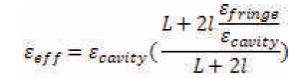
The effective dielectric constant can be calculated in the mixed air-silicon region which is just at the bottom of the patch. The effective capacitance is given by,
where,
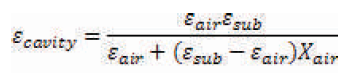
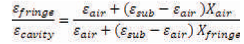
In the above expressions, A is the area of the patch and t is the thickness of the substrate. e represents the relative cavity dielectric constant of mixed substrate region and e fringe represents the relative dielectric constant in fringing field region. The thickness parameters x and x are the air fringe ratios of air to full substrate thickness in the mixed and fringing field regions, respectively. L is the patch length and l is the open end effect extension of patch (Papapolymerou et al., 1998; Prasad and Chattoraj, 2013).
Figure 2 shows the variation of effective dielectric constant with percentage change of air gap thickness for Si substrate (e=11.9) with three different open end effect r extension percentage of the patch.
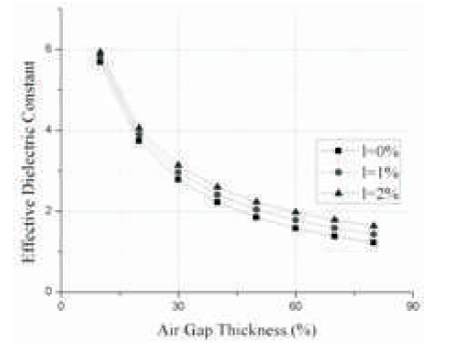
Figure 2. Effective Dielectric Constant vs Air Gap Thickness (%) plot
The MEMS switch used in this design is cantilever type and electro-statically actuated. The overall dimension of the switch is 100 X 400 mm . The switch membrane is suspended over the microstrip line. The switch membrane is made of low stress nitride layer of 1 mm. At the tip of membrane, Gold (Au) of thickness 0.5 mm is deposited (Basak et al., 2005; Ramola and Pearson, 2013). The details of the switch are given in Table 1.
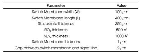
Table 1. Details of the RF Switch
Two actuation pads are lying on the base of the switch, and one actuation pad is on the top of the switch membrane which is made of Au of thickness 0.5 mm. The actuation voltage pulls the switch in down state and the secondary patch is associated with the main patch. Figure 3 shows the structure of a MEMS switch. Six-inchhigh resistive silicon wafer will be processed in the foundry. The Plasma-enhanced Chemical Vapor Deposition (PECVD) will be used for oxide and nitride deposition, and wet or dry etching for switch release.
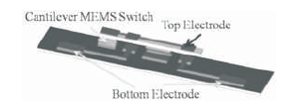
Figure 3. The Structure of MEMS Switch
The spring constant (k) of fixed beam cantilever switch is given by (Prasad and Chattoraj, 2013; Rebeiz and Muldavin, 2001; Weedon et al., 2001),
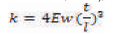
where, E is the spring constant of Silicon Nitride (SiN) (210 GPa), w is the membrane width, t is the membrane thickness and l is the switch length. For this design, the spring constant is 13.12, as calculated from equation (5). The pull in voltage (V ) of the cantilever switch is given by p (Rebeiz, 2004),
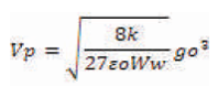
where, e is the dielectric constant of air, W is the o transmission line width, g is the gap between switch o membrane and t-line, when the switch is in OFF state.,
In Figure 4, pull-in voltage of MEMS switch with respect to the air gap of the switch is plotted. The simulation is executed in CoventorWare 2010 simulator. The plot shows the actuation voltage to be 15.6 V. The residual stress of the switch is expected to be, 10 MPa provided by foundry and it has been incorporated in the simulation. The return loss of the patch in both of the switch states is about 20 dB at the desired resonance frequencies, which is shown in Figure 5.
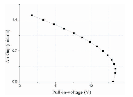
Figure 4. Pull in Voltage Plot of a MEMS Switch
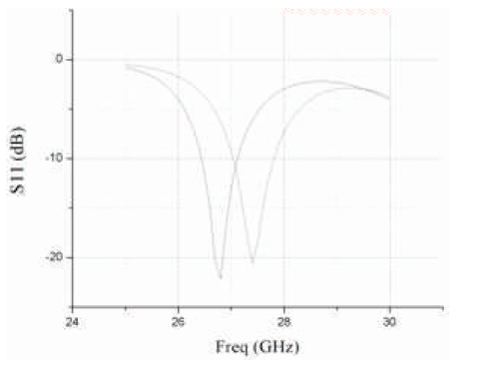
Figure 5. Return Loss of Designed Configurations
Frequency response of the reconfigurable radiator depends on the switching state of MEMS. The simulation is performed in High Frequency Structure Simulator (HFSS) simulator. As Radio Frequency (RF) switch is in OFF state, minimum S occurs at 27.4 GHz and shifts 26.8 GHz, as the 11 switch is turned ON.
The simulated far field radiation patterns are shown in Figure 6. The 2-D plot of gain is shown in Figure 7. The simulated gain is 4.2 dBi for 60% of substrate etching at o θ=0 . Figure 8 shows the 3-D plot of antenna gain, and it is observed that there is no variation in gain pattern at the two resonance frequencies. Thus, it is concluded that there is reconfigurability in terms of frequency only. The variation in Bandwidth (BW), Resonance Frequency (F ) C and Return Loss (S ) with change in substrate etching for 11 two different conditions, i.e. (i) MEMS switch OFF and (ii) MEMS switch ON, were simulated and shown in Tables 2 and 3, respectively.
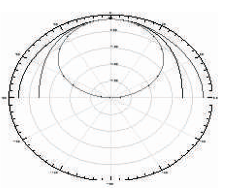
Figure 6. Far Field Radiation Patterns of the Design
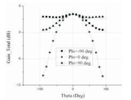
Figure 7. Rectangular Plot of Gain
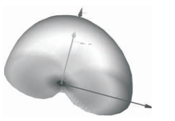
Figure 8. 3-D Plot of Gain
Comparison of Tables 2 and 3, implies the best possible result with 50% etching. Figures 9 and 10 show the return loss plots with change of etching.
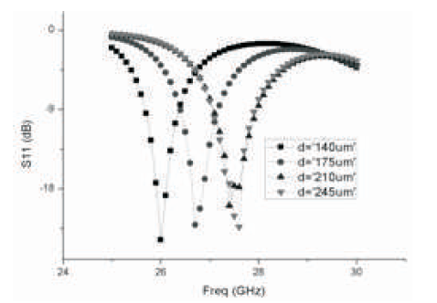
Figure 9. Change in Resonance Frequency with Change in Etching (MEMS switch OFF)
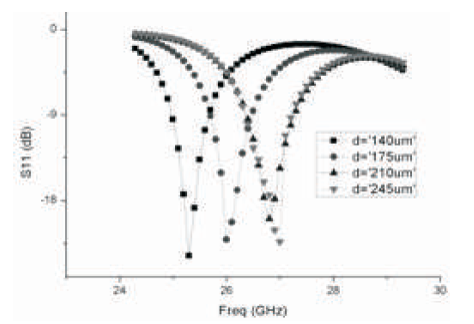
Figure 10. Change in Resonance Frequency with Change in Etching (MEMS switch ON)
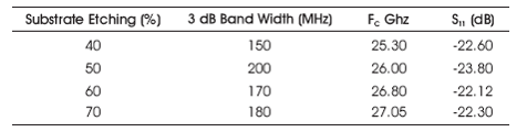
Table 2. Variation of BW, F and RL with Substrate C Etching with MEMS Switch ON
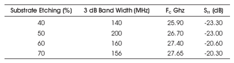
Table 3. Variation of BW, F and RL with Substrate C Etching with MEMS Switch OFF
The design of a frequency reconfigurable antenna using the ON/OFF state properties of an electo-statically actuated MEMS switch is presented in this paper. This approach describes the design and simulation of reconfigurable patch using cantilever type MEMS switch on high resistive Si substrate. To minimize the space constraint, same substrate is utilized for the radiator also. In this design, two radiators are connected via a MEMS switch, and depending on the position of the switch, the resonance frequency is reconfigured. The change in bandwidth, return loss and resonance frequency are simulated with variation in etching depth. The pull-in voltage is 15.6 V including the residual stress factor. The simulation shows a shift of 600 MHz in resonance frequency and change of bandwidth of 50% with etching, with a gain of 4.2 dBi. This design is having a potential in Package type of application systems. It can also be concluded from the result that there is reconfigurability only in frequency; however, the gain and radiation patterns remain unchanged at the operating frequencies.
The authors are grateful to the Director, SAC and Deputy Director, SNPA and Group Director, ODCG, SNPA for completing the work. The authors would also like to thank the management of Nirma University, Ahmedabad, India for providing the necessary support and encouragement.