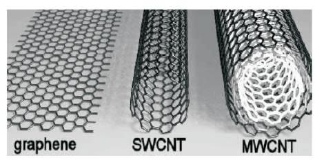
Figure 1. Structure of Grapheme Sheet, Single Walled CNT and Multiwalled CNT
Many research groups attempt to extend Moore's law for digital circuits beyond the expected end of the CMOS scaling by proposing alternate devices. Designing MOSFETs with channel lengths much smaller than a micrometre is a challenge, and creates the problems in device fabrication, which limits advancing the integrated circuit. Small size of the MOSFET, below a few tens of nanometres creates the low Trans-conductance, gate oxide leakage, low On-current, Mobility degradation and increased delay. Problems observed in the MOSFET when size is reduced are avoided in CNTFET, since in case of CNTFET carbon nanotube is used as channel and high-k material is used as gate dielectric and also our result shows that CNTFET exhibit the better performance than MOSFET in current conduction. In this paper, the authors present the spice model creation of MOSFET like CNTFET, current-voltage characteristics of an emerging nano device with classical behavior MOSFET like CNTFET. Specifically, they have concentrated on semiconducting carbon nanotube field effect transistor (SCNTFET). Device has been simulated using spice and also they investigate the performance of digital inverter gates based on semi-conducting CNTFET.
The last few decades metal oxide semiconductor field effect transistor (mosfet) size has continually been reduced,and this size reduction increase the number of transistors on chip or chip with more functionality in the same area. It is also expected that small transistor switches faster. Designing of MOSFET with channel length much smaller than a micrometre is a challenge, and creates the problems in device fabrication, which limits advancing the integrated circuit. Small size of the MOSFET, below a few tens of nanometres creates the low Transconductance, gate oxide leakage, low on-current, Mobility degradation, increased delay. When the size of MOSFET is below a few tens of nanometers the semiconductor industry is starting to face several difficult challenges. Scaling has resulted in increased shortchannel effects, reduced gate control, exponentially rising leakage currents, severe process variations, and unmanageable power densities.
Therefore, alternative technologies to bulk silicon transistors are being explored, One of such a device is Carbon nanotube field effect transistors (CNTFETs), which utilize semi conducting single-wall CNTs to assemble electron devices similar to MOSFETs, and fabrication of CNTFETs has been reported in recent years. Also, a CNTFET has a significantly smaller off current; therefore the power consumed when the transistor is off is greatly reduced in CNTFET designs. These properties make CNTFET one of the promising new devices to extend or complement tradition silicon technology for high performance and low power design [1][2].
Carbon nanotubes are formed, when a graphene sheet of a certain size that is wrapped in a certain direction [3]. As the result is cylinder symmetric we can only roll in a discreet set of directions in order to form a closed cylinder. Two atoms in the graphene sheet are chosen, one of which servers the role as origin. The sheet is rolled until the two atoms coincide. The vector pointing from the first atom towards the other is called the chiral vector and its length is equal to the circumference of the nanotube. The direction of the nanotube axis is perpendicular to the chiral vector. SWNTS with different chiral vectors have dissimilar properties such as optical activity, mechanical strength and electrical conductivity [4]-[6], [13]. In Figure 1 the structure of graphene sheet, Single-Walled CNT and a Multi-Walled CNT is shown.
The transistor configurations based on single walled carbon nanotubes (SWNTS) are various: the Schottky barrier CNTFET (SB-CNTFET) [7] [12], the conventional CNTFET (c-cntfet) featuring a doping profile similar to n- MOSFET[8] the dual-gate CNTFET, exhibiting n- or p-type unipolar behavior tunable by electrostatic doping [9] and the tunneling CNTFET [10] [13] .The subject of this paper is the conventional CNTFET. Its structure albeit simple provides a behavior like normal MOSFET with yet ballistic transport [11]. In this device, depicted in Figure 2 the ungated regions (source and drain regions) are heavily doped and it operates on the principle of barrier-height modulation by application of the gate potential.
In this case, the on-state current is limited by the amount of charge introduced in the channel by the gate and, for source-drain distances shorter than 150nm, the transport is assumed to be free of significant scattering and thus essentially ballistic at both high and low voltages. Hence, the description of current flow through the CNT lies on (i) the features of ballistic transport and (ii) the specific electron confinement along the tube circumference[14].
Figure 1. Structure of Grapheme Sheet, Single Walled CNT and Multiwalled CNT
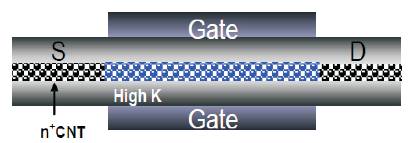
Figure 2. Structure of Carbon Nanotube Transistor Configuration
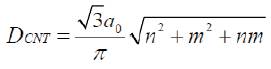
Carbon nanotube field effect transistors (CNTFETS) utilize semi conducting single-wall CNTS to assemble electronic devices. A single-wall carbon nanotube (or SWCNT) consists of one cylinder only, and the simple manufacturing process of this device makes it very promising for alternative to today's MOSFET. An SWCNT can act as either a conductor or a semiconductor, depending on the angle of the atom arrangement along the tube. This is referred to as the chirality vector and is represented by the integer pair (n, m). A simple method to determine if a carbon nanotube is metallic or semiconducting is to consider its indices (n, m): the nanotube is metallic if n=m or n-m=3i, where, i is an integer. Otherwise, the tube is semiconducting. The diameter of the CNT can be calculated based on the following equation [17].
where,
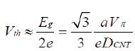
a0= 0.142 is the inter-atomic distance between each carbon atom and its neighbor. similar to the MOSFET device, the CNTFET has also four terminals. The currentvoltage (I-V) characteristics of the CNTFET are similar to MOSFET's. The threshold voltage is defined as the voltage required to turn on transistor. The threshold voltage of the intrinsic CNT channel can be approximated to the first order as the half band gap that is an inverse function of the diameter [17].
where,
a = 2.49 Å is the carbon to carbon atom distance, Vπ = 3.033 eV is the carbon π-π bond energy in the tight bonding model, e is the unit electron charge, and DCNT is the CNT diameter. As DCNT of a (19, 0) CNT is 1.487 nm, the threshold voltage of a CNTFET using (19, 0) CNTs as channels, is 0.293v, The device channel consists of a (19,0), zigzag CNT with a band gap of 0.53 eV and a diameter of 1.5 nm. The device cross-sections are shown in Figure 2 which is the cross section of a C-CNTFET. The gate dielectric is a 2nm thick HfO2 (k = 16) and the device has channel length of 100nm.
For the above mentioned device configuration the electrostatic drain capacitance CDE = 0.1 aF and electrostatic source capacitance CSE = 0.7 aF; gate resistance RG = 10 Ω; and temperature T = 300 K.
Transconductance of the CNTFET is can be calculated as Follows
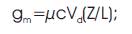
μ is the carrier mobility, c is the gate capacitance, Vd is the drain voltage, Z is the channel width and L is the channel length for the simulated device the transconductance is 14.1mS when gate capacitance is 532pf, Table 1 shows the various parameters required to create the CNTFET model in PSPICE[15] [17].
This paper presents simulation SCNTFET based inverter circuit simulation in PSPICE and also gives the current – voltage characteristics of CNTFET for the given sourceand drain voltage, Figure 3 shows drain current as a function of gate voltage and when drain voltage is 1v, Figure 4 shows the simulation result for drain current as a function of drain voltage and various gate voltage VGS = 0.4v, 0.6v, 0.8v, 1v and Figure 5 shows the Scntfet based inverter circuit with resistive load.
In this paper semi-conducting CNTFET based inverter with resistive load are simulated in pspice and simulation results are shown in Figure 6. In this simulation nanotube length is 100nm. Performance of CNTFET in current conduction is high due their high gate capacitance; this high capacitance value increase on state current of the device, gate capacitance value is increased by using high-k dielectric material as gate dielectric.
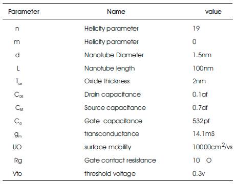
Table 1. CNTFET Parameters
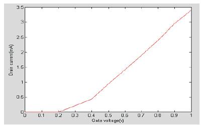
Figure 3. Drain Current Ids as A Function of the Gate Bias for Vds = 1v
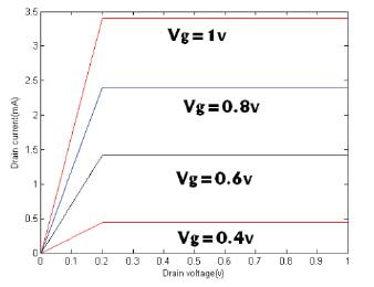
Figure 4. Drain Current Ids as a Function of the Drain Bias for Vgs = 0.4v, 0.6v, 0.8v, 1v
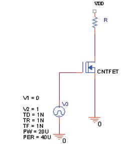
Figure 5. Semi-conducting CNTFET Based Inverter with Resistive Load
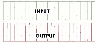
Figure 6. Simulation Results for Semi-conducting CNTFET Based Inverter with Resistive Load
In this paper we have analyzed the CNTFET model creation in pspice and current conduction of the CNTFET and Drain characteristics shows the drain current variation in SCNT. Drain current gets saturated after 0.2v, and SCNT gives high On state current and this will make replacement of the MOSFET by CNTFET for the future nano devices.