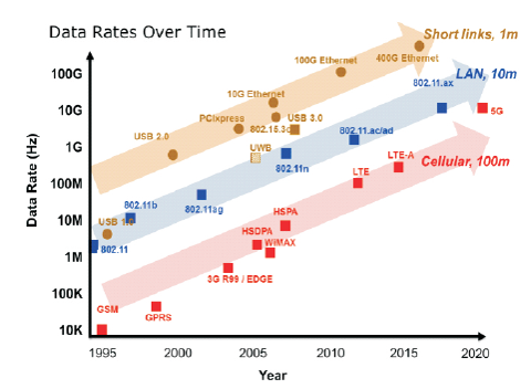
Figure 1. Data Rate Trends in Wired, Wireless and Cellular Communication Standards [27]
The aim of this review paper is to define the role of SiGe HBTs within the Technology Revolution that will lead to a globally interconnected smart world. At first, the authors have presented the recent developments of SiGe BiCMOS technologies and their applications to unit circuit blocks and integrated solutions. Then modern HBT device structures, technological aspects, scaling strategies, design issues, and future directions are also discussed. TCAD-based simulations predict that SiGe HBTs with cut-off and maximum oscillation frequencies of 780 GHz and 2 THz, respectively will become feasible by the year 2030.
“Intelligent chips for a smart world” was the topic of the International Solid-State Circuits Conference (ISSCC) 2017 [27], where recent advancement in solid-state circuits and systems-on-chip has been presented, outlining the central role that SiGe HBTs play within the evolutionary process that will lead to a globally interconnected world. Current advancement in SiGe HBT technology is the result of several years of steady research studies and progress from the initial material preparation in 1984, through device demonstrations from 1987-1992 to commercial product in 1996 [1], that have paved the way to the development of silicon-based THz systems. The reason that has driven researchers to investigate in silicongermanium alloys properties must be sought with the aim of extending band-engineering techniques, already well experienced in III-V compound semiconductors technology, to silicon in order to overcome the BJTs “base dilemma” and exploiting low-cost, high-integration and excellent thermal properties of silicon [41]. Since the first report of SiGe HBT in 1987 [29], there has been tremendous progress in SiGe research, leading to the achievement of cut-off and maximum oscillation frequencies (f /f ), of 505 GHz and 720 GHz, respectively T max [23]. Today Si-Ge HBTs represent a milestone for the practical implementation of new technologies aimed to ensure the progress goes ahead.
Concurrently with HBT technology advances, a large variety of electronic and optoelectronic devices based on SiGe alloys have been developed. Whether in bipolar applications lattice mismatch between silicon and silicon-germanium alloy must be kept under control in order to avoid the occurrence of misfit and threading dislocations, strained silicon channels grown over relaxed SiGe buffers improve device performance in MOSFETs due an increase in hole and electron mobility [46], [69]. Under 90 nm technology node and beyond, the achievement of performance improvements through the device scaling, such as reducing the gate length and thinning the gate oxide is anything but simple due to the onset of second order effects [50]. Strained-Si channels is one of the so-called “technology boosters” aimed to improve MOSFET performance with the same lithography feature. For instance, applying tensile strain to a nchannel MOSFET leads to a mobility enhancement due to the increase in the occupancy of electrons in the two folds valley and the suppression of inter-valley scattering. Improvements in mobility of p-channel MOSFET resulting from the application of uniaxial compressive strain are due to the reduction in effective mass of occupied bands and the suppression of inter-subband scattering. Two types of mechanical stress have long been investigated, biaxial stress [26] and uniaxial stress [64]. Better performance have been achieved introducing uniaxial strain into channels locally inside MOSFETs. Through selective epitaxial deposition of SiGe in recessed/raised source and drain techniques current improvements ranging in 60-90% have been reported [5], [12]. Depositing a high-compressive SiN cap on top of SiGe could enhance mobility by 200%. Uniaxial process induced-stress has made silicon a high-mobility semiconductor, competitive with un-strained III-V materials. This could play an important role in the development of high-performance ICs based on SiGe BiCMOS technology.
Exploiting these advantages, strained-Si channels on relaxed SiGe n-MODFETs [14], [74] and strained SiGe on relaxed Si or strained Ge on relaxed SiGe p-MODFETs [24], [40] have been demonstrated. In optoelectronic field, research efforts have been focused on the development of components for 1.3÷1.55 μm fiber optic communications and 3-5 μm telecommunications. Photodetectors [42] and light-emitting diodes [44], based on SiGe, with a response in 1.3-1.55 μm have been demonstrated. The main goal of investigating in SiGe optoelectronic capabilities is the development of a Sibased optoelectronic integrated circuit consisting of the analog/digital section based on SiGe BiCMOS technology and the optic side, comprising SiGe based emitters and detectors, interconnected through SiGe optical waveguides.
In this review paper at first the authors discuss about the motivations behind the emergence of new high data rates communication standards, such as IEEE 802.2 400 Gb/s, LTE-A and 5G, contextualizing the role that SiGe HBTs will play for the development of integrated systems suitable for these emerging applications. Then they present an overview of recent advancements in SiGe BiCMOS technology through the discussion of recently reported unity circuit blocks and integrated solutions operating beyond 100 GHz. Moreover modern SiGe HBTs structures and technological aspects are discussed together with design tradeoffs and scaling strategies implemented by some of the most important foundries all over the world. At last future trends and TCAD predictions are outlined.
Today, all around us there are signs that we are entering a new era, of unprecedented technological changes, characterized by the sharing of a large amount of data among people and various interconnected smart devices through the internet. The incoming of the smart world era is driven by the Internet of Everything (IoE) tendency that relates the intelligent connection of people, processes, data and things through internet to improve business and industry outcomes and ultimately make people's life better. The IoE represents an enhancement to the Internet of Things (IoT), where interconnected smart devices share informations and interact with the external world making intelligent decisions. In other words, the purpose of the IoE is the full integration of people's life and smart devices in a truly smart and interconnected world.
The networking company Cisco has estimated that around 50 billion devices would be interconnected and exchanging information by 2020 [13].
Figure 1 shows the data rate trends in wired, wireless, and cellular communication standards.
Figure 1. Data Rate Trends in Wired, Wireless and Cellular Communication Standards [27]
As it can be seen, data rates increase of about 10 times every 5 years. The IoE revolution is bringing an explosion of demand for network bandwidth. Everything will be connected through wired and wireless networks, generating a tremendous amount of data to be processed and analysed in the cloud. The lack of spectrum in traditional frequency band has made necessary to look for higher frequency spectrum to find large amount of continuous bandwidth in order to address the significant growth in wireless broadband traffic and future high speed and low latency applications. This is the reason that has driven the d e v e l o p m e n t o f e m e r g i n g h i g h d a t a r a t e s communication standards, such us IEEE 802.3 400 Gb/s, LTE-A, and 5G that targets 10 Gb/s to 100 Gb/s, that will allow the smart world to take shape. This ongoing fusion between real world and virtual world is the result of several years of studies research and progress in semiconductor electronic devices operating in the THz region that has led the development of integrated systems with adequate per formance to meet emerging applications requirements. For high data rates communication standards, significant enhancements in architecture, bandwidth and operation frequency of transceivers and fiber optic systems are needed.
Figure 2 shows a typical cellular station (or point to point radio receiver) and a typical optical fiber and active optical cable module [13].
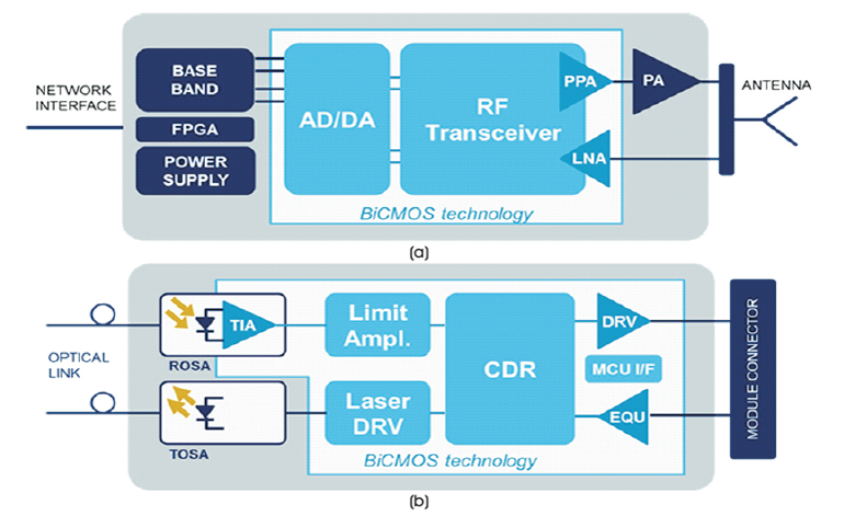
Figure 2. (a) Typical Cellular Station or Point to Point Radio Receiver, (b) Typical Optical Fiber and Active Optical Cable Module
SiGe HBTs will play a central role in the development of the Analog and Mixed Signals (AMS) of these devices due to the advancements in SiGe technology that have made silicon a viable low-cost solution for advanced wireless and wireline communication systems operating at sub mm-wave frequencies, such as 5G handsets, IoT devices, high-speed data networks, and data center communications. Furthermore, SiGe BiCMOS technology allows the easy and cost effective integration with advanced CMOS and on chip passive, providing efficiently system on chip integration. It is not coincidence that foundries are continually making efforts to improve their SiGe technology process. Recently STMicroelectronics has shown a 55 nm SiGe BiCMOS technology reaching values of f and f about 320 GHz and 370 GHz respectively [21]. T max Modifying its 0.18 μm BiCMOS process and implementing a fully self-aligned double poly solution, NPX Semiconductors has achieved values of f and f about 230 GHz and 400 GHz, respectively in a 90 nm BiCMOS process [65]. IBM has shown a 90 nm BiCMOS technology reaching values of f of 300 GHz and f about 360 GHz T max [48]. TowerJazz has optimized its 0.18 μm SiGe BiCMOS process achieving a third generation technology suitable for building transceivers for next generation wireless and wireline communication standards, 100 Gbs and 400 Gbs Ethernet and 5G cellular data networks, exhibiting values of 240 GHz for f and 280 GHz for f in a cost-effective and T max analog-friendly 0.18 μm node [52].
The highest value of f has been reached by IHP using a max 0.13 μm BiCMOS technology showing values of f and T fmax up to 300 GHz and 500 GHz, respectively.
The adequate technological maturity reached by SiGe has made possible the development of a large number of building blocks, such as high gain and low noise power amplifiers, oscillators, mixers, and fully integrated transceivers operating beyond 100 GHz, demonstrating that SiGe BiCMOS technology represents a keystone for the practical realization of ICs capable of meeting emerging application specifications.
Recent improvements in SiGe HBT technology have paved the way for the development of integrated systems suitable for various THz applications, including broadband communications and high-resolution imaging. In this section, recently reported unit circuit blocks and integrated solutions, based on SiGe HBT technology, operating at mm-wave frequencies will be briefly discussed.
Amplifiers play a central role in high frequency systems. They are largely used at the received side for reducing the overall noise level of the system and for the final boost of output power at the transmitted side. Amplifiers are also inserted in multiplier chains to compensate for power loss during frequency conversion processes. High frequency amplifiers design demands stringent requirements for the maximum HBT operation frequencies, f and f , since a T max sufficient gain needs to be guaranteed at the target frequency. Considering the typical transistor RF characteristic that exhibits a gain roll-off of -6bB/octave, the loss of passive components used for matching and possible process variations, the required f should be max about two/three times greater than the operation frequency of the amplifier in order to meet the required gain. From this point of view, the needed of high performance amplifiers operating in the THz region drives research in SiGe HBTs with ever higher values of f and f .
The highest operation frequency of SiGe amplifiers recently reported is up to 260 GHz [53]. It has been implemented using a three-stage differential cascode topology, fabricated with IHP 0.13 μm SiGe technology with f /f of 350/500 GHz. The design of amplifiers T max operating beyond 200 GHz is challenging not only due the limited gain achievable at these frequencies, but mostly due to the onset of stability issues. The reported amplifier [73] implements a passive shunt transistor pairs at the output of each amplifying stage, as stability tuning units, to overcome instability caused by parasitic base inductance of the three Common Base (CB) stages, as shown in Figure 3.
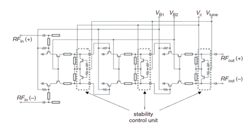
Figure 3. Schematic of the Differential Amplifier
The stability of the amplifier can be adjusted through apost fabrication tuning procedure, varying the base bias that leads a variation of the input impedance of transistors. With a reported gain of 15 dB at 260 GHz and a 3-dB bandwidth of 16.5 GHz, the amplifier shows great performance for use in broadband communications and THz imaging systems.
Low Noise Amplifiers (LNA) are generally employed at the first stage of receivers or detectors, since this technique reduces the overall noise level of the entire RF system. Modulation formats, adopted in new high data rates communication standards, such us 400 Gb/s and 1 Tb/s fiber optic link, calls for the development of high speed low noise amplifiers. The challenge in the development of LNAs suitable in these systems is the simultaneous achievement of high operation frequency, high linear input range, low Noise Figure (NF), and high gain. Recently reported LNAs based on SiGe technology show NF values of 9.6 at 122 GHz [70], 7.7 at 130 GHz [75], and 6.2 at 140 GHz [71] with gains ranging in 13-30 dB.
An interesting LNA suitable for time-interleaved 120 Gb/s fiber optic receiver has been recently reported [25]. Based on STMicroelectronics 55 nm SiGe BiCMOS technology with f /f of 350/500 GHz, the amplifier shows T max a figure noise less than 7 dB up to 88 GHz, a linear input range of 800 mV and a gain of 8.5 dB with a 3 dB pp bandwidth of 135 GHz. Fiber optic applications require a low-noise, linear front-end capable of amplifying the fullbandwidth input signal. The challenge in design of LNAs suitable for high datarates fiber-optic communications is the simultaneous achievement of low FN, a wide linear input range, and a large bandwidth, still providing a decent gain. The amplifier proposed is a 5 stage DC coupled single ended distributed amplifier. Each of the five stages is implemented using MOS-HBT cascode configuration, as shown in Figure 4 [25].
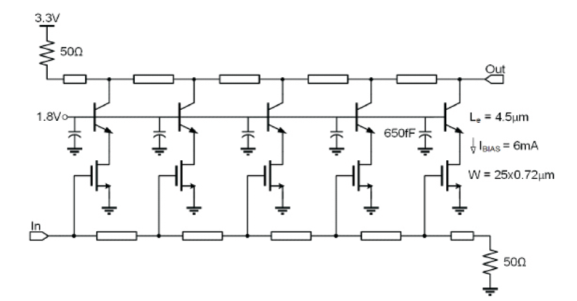
Figure 4. Schematic of the 5 Stages Distributed Amplifier
The achieved wide linear input rage is mostly due to the distributed topology that leads the widest possible bandwidth for a given technology. The single ended MOSHBT cascode topology leads a great DC coupling to the input line since the higher Q impedance of the gate of the MOSFETs than that the HBTs. This allows the avoidance of unnecessary power consumption due to shunt losses. Furthermore, a cascode topology offers higher gains than that common-source and common emitter stage configurations. The distributed amplifier occupies 0.36 2 mm for the core area with DC power dissipation of 99 mW. The results achieved represent a step forward toward the development of integrated transceivers for next generation 1 Tb/s optical-links.
Power Amplifiers (PA) are generally placed at the first stage of transmitters, which leads the achievement of high Signal-to-Noise (S/N) at the receiver or detector side. The challenge in the design of these amplifiers is the simultaneous achievement of high output power and high operating frequency. Advanced SiGe technologies delivers transistors with high values of f and f and low T max noise adopting high collector doping concentrations that leads to small breakdown voltages of these transistors, limiting the HBTs output power. The needed of high performance PAs, drives the improvement of cut-off frequency and breakdown voltage trade-off in future SiGe HBT technology nodes. Recently, saturated output power (P ) values of 20.8 dBm [38], and 22 dBm [15] have been sat reported in 90 nm SiGe technology at 116 GHz and 120 GHz, respectively. Both amplifiers use the 8-way power combiner configuration. Reported values of saturation output power decrease as the frequency increases, falling to 10 dBm [56] and 11 dBm [2] at 160 GHz. The highest reported output power for PAs above 150 GHz is up to 15.5 dBm at 160 GHz using IHPs 130 nm SiGe BiCMOS technology with values of f and f equal to 250 GHz, and T max 300 GHz respectively [20]. The amplifier has been implemented using 4 driving stages based on wideband cascode amplifiers and a high output stage. Optimizing the HBTs size in the power stage and operating in the weak inversion region, values of P of 15.5 dBm and PAE of 7.2% sat have been achieved at 160 GHz. In order to provide a peak differential gain of 30 dB, has been implemented an inductive positive feedback on the common-base output stage. The drawback associated to this technique concerns stability issues as discussed previously.
Oscillators play a crucial role in THz systems design since the needed of high power signal sources critically demands high-performance oscillators operating in this frequency region. Furthermore, oscillators are an indispensable component for heterodyne systems in both receivers and transmitters that is required to provide local oscillation to the mixer. Voltage Controlled Oscillators (VCOs) are the most widely used type of oscillators in SiGe RF systems operating beyond 100 GHz since the frequency tuning capability is useful for various purposes including Phased Locked Loop (PLL) applications, as well as, the compensation of oscillation frequency shift due to process variations. Although VCOs design at high frequencies is fairly challenging, due the relative low power output, high phase noise and low frequency tuning range achievable in the THz region, it is less complex than amplifiers design at the same frequencies. The reason is that a gain slightly greater than unity is enough to trigger oscillation. This makes possible the implementation of circuits operating near f of the device. Furthermore, the max oscillation frequency can be further increased by taking harmonic signals as the output instead of the fundamental signal. In general, the n-push technique can be used to take the umpteenth harmonic from the oscillator. This provides an oscillation frequency much higher for a given technology process than that the maximum operation frequency at which amplifiers can work. For this reason, during these years, have been reported SiGe oscillators based on multiplication techniques such as doublers [6], [37], [59], push-push [6], [45], [67], [68] and triple [11] reaching values of oscillation frequency up to 300 GHz at the price of a low efficiency about 0.07% (39), and DC power consumption that exceeds hundred milliwatts [11].
A main drawback of such techniques is related to the poor spectral purity of the output signal due the anything but simple complete suppression of the fundamental and other harmonics generating during the up-conversion process. Furthermore, using frequency multiplication increases power consumption ad degrades phase noise by 20logN, where N is the multiplication factor.
Fundamental wave oscillator’s design is typically more challenging with respect to phase noise performances and tuning range, since the Q passive and transistors gain decrease as the frequency increases. Numerous SiGe VCOs implementations based on fundamental mode operating beyond 100 GHz have been recently reported [3], [30], [31], [76]. The highest frequency reached by fundamental mode VCOs is up to 240 GHz [3]. The VCO, fabricated in a 130 nm SiGe BICMOS technology with f /f T max of 250/270 GHz, is capable to drive directly a divide-by-8 dynamic frequency divider chain that provides a single ended power of -11.5 dBm. It shows a relative high tuning range of 229 - 240 GHz and a phase noise of -78 dBc/Hz at 1 MHz offset. The reported DC power dissipation is of 97 mW.
Mixers are a key circuit block in RF transceivers that perform the down conversion of the RF signal to intermediate frequency band or the up-conversion of the IF signal to the RF band. Active mixers are preferred for most applications since they help to suppress the noise from the following stages and add gain to the system total gain. There have been several reports of mixers based on SiGe technology operating beyond 100 GHz. The main challenge in design of mixers operating at these frequencies is the simultaneous achievement of high conversion gain, low noise, high linearity still maintaining low DC power dissipation levels. Furthermore, VCOs output power tends to decrease as the frequency increases and could not be sufficient to drive the mixer directly. Mixer design should achieve high conversion gain and allows less stringent LO power requirements. The most popular adopted configuration is the Gilbert cell topology. Mixers based on Gilbert cell show large values of DC power dissipation, reaching several tens of mW or higher [51], [57]. Considering the ever more stringent constrains in terms of power dissipation imposed in the high-speed circuits design and since passive mixers are available free of extra power consumption, such a level of power dissipation is not tolerable in design of mixers operating at mm-wave frequencies. Mixers based on Gm-boosting represent a valid alternative for the development of low power circuits, improving the performance of gain stages with modest power consumption. Different Gm-boosting methods have been proposed in these years. Great performances have been achieved using self-switching common-base topology with capacitive cross coupling, in which the Gmboosting method is applied to both RF and LO stages in order to enhance the input signal and reduce LO power level [18], [33], [34]. High values of conversion gain of 11.5 dB have been reached [34] showing very low DC power consumption levels around 1.5 mW [33] at 135 GHz, at the price of relatively high LO power, up to 10 dBm.
Recent Si-based circuit design techniques improvement have paving the way to the implementation of integrated THz circuits. The challenge in integrated circuit development operating at these frequencies is the precise matching between unit circuit blocks since as the frequency increases the mismatch due little process variations in passive components leads to a significant design errors. A large number of integrated systems, based on SiGe HBT technology, operating at mm-wave frequencies, for THz imaging [22], [32], [62], [72], Frequency-modulated Continuous Wave (FMCW) RADAR [19], [21], [36], and high data rates communications [17], [39], [54], [56] have been recently reported showing good performance in terms of integration level and power consumption. The fifth generation (5G) communication is attracting interest worldwide since the recent explosion of mobile data traffic that will lead us towards a new era where everyone and everything will be connected. Current networks cannot satisfy the associated bandwidth demand [4]. On account of this, efforts are being made all over the world to design new wireless technologies that will support the expected demands for the next decade. 5G aims to provide improvements in data rates, latency, and link robustness. Since the saturation of the benchfront spectrum, mm-wave spectrum represents a valid opportunity to address the incoming bandwidth requirements due the vast amount of idle spectrum in range 30-300 GHz. This portion of spectrum has remained unused so far due hostile propagation qualities, strong phase noise, but the most important because of the exorbitant and prohibitive equipment cost. The recent advancement in SiGe HBT technology have made silicon a valid low cost alternative to conventional III-V material compounds for the development of integrated systems operating at mm-wave frequencies, much that, almost certainly, SiGe HBTs will replace GaAs HBTs in future mobile transceivers. A main issue for the development of 5G networks concerns antennas design. Since considerable free-space path loss at mm-wave frequencies, massive MIMO technology is the most appropriate technology since it allows aggregating multiple antennas, with different apertures, into a multi-cell array. The challenge is co-phasing these antennas so that they steer and/or collect energy productively. This problem becomes more severe when the channel changes rapidly for instance due to mobility or due to rapid alternation in the physical orientation of the device. This demands multiple and reconfigurable polarizations with directional fan-beam radiation pattern antennas. Therefore, the challenge for the development of 5G pico-cells or mobile transceivers is the implementation of an Antenna in Package (AiP) solution, capable to support a large number of precisely controlled beams, providing high output power with low DC power consumption.
An interesting integrated 32-element phased-array transceiver, operating at 28 GHz, suitable for 5G communication, has been recently proposed by IBM [54]. Implemented in 0.13 μm SiGe BiCMOS technology, the system includes two independent 16-element phased array enabling two concurrent and independent 16- element beams in either transmission (Tx) or reception (Rx) mode. The IC transceiver implements an RF phase shifting architecture in order to minimizing the number of circuit components resulting in a compact solution of 15.6 x 10.6 2 mm . Phase-array adopts 8 x 2 combining/splitting signals architecture instead of a more efficient 16 x 1 solution [54]. Two sets of 8 signals are fist combined/splitting at 28 GHz using a Wilkinson divider, then are further combined/split at the 8 GHz internal IF. Improvements achieved in terms of linearity due the reduced number of signals handled by RF mixers come at a cost of an extra mixer per path.
Moreover in the Tx/Rx switch, proposed by IBM [54], compared to a classic Tx/Rx switch configuration, the λ/4 tline based switch at the power amplifier side has been removed. This allows the reduction of insertion loss in transmission mode of 1.2 dB resulting in an increase in the saturation output power (P ), reaching a P value of 16 sat sat dBm per signal path and a power amplifier efficiency greater than 20%. In terms of power consumption that means a DC power saving of 2.35W. Improvement in Psat comes at a cost of a decrease of only 0.6 dB in Noise Figure (NF) in received mode. The reason why Rx performance does not result strongly degraded is the use of switched capacitors to resonate out the inductive part of the transmission stage input impedance. This leads a high Tx input impedence at the antenna, maximizing the Rx signal flow into the low noise amplifier.
Figure 5 [54] shows the 43 different 16-element beams across ±30° range, obtained during beam forming test using an antenna in package module with 4 ICs and 64 dual polarized antennas.
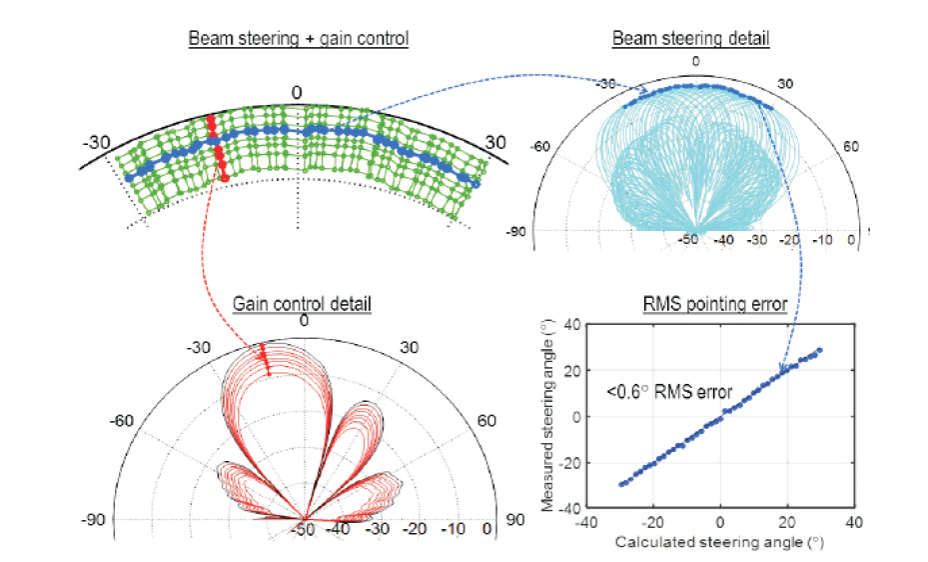
Figure 5. 16-element Beam Steering Across ±30° Range
The peculiarity of the reported transceiver is that it supports concurrent and independent dual-polarized operation in Tx and Rx mode leading in a further degree of freedom in beam steering. A resolution of 1.4° with an error across of all directions of 0.6° RMS has been achieved, resulting in a high directional capabilities and great gain control. Being antenna-in-package array compatible, with high beam forming capabilities and high gain control, the reported transceiver represents a great step forward for development of future 5G pico-cells.
SiGe Heterojunction Bipolar Transistor devices are bipolar junction transistors created using a thin epitaxial base incorporating a germanium mole fraction ranging in 8- 30%. This modification tremendously improves device performance allowing the extension of band gap engineering techniques to silicon.
Two main approaches are used in SiGe HBT design, uniform germanium profile, and graded germanium profile. SiGe HBTs adopting a uniform Ge base profile, implement a wide gap emitter structure having the peculiarity that the majority of the band gap difference between SiGe and Si occurs in the valence band, leading to an increase in the efficiency of electron injection into the base, while the efficiency of holes remains unchanged compared to a silicon homojunction. The imbalance in charge carriers efficiency injection is the key feature that allows to overcome the BJTs base dilemma and leads to the achievement of a gain enhancement. For a silicon BJT better RF performance can be achieved reducing the base width, that leads to an improvement in base transit time [50]. The mechanism that limits the extend that the base width can be reduced is the punchthrough of the base, that can be avoided increasing the base doping concentration. The main issue associated with this technique is that increasing the base doping degrades the current gain. The high current gain achievable in a SiGe HBT can be treaded off for increasing the base doping or lower emitter doping to improve base resistance and the emitter-base capacitance leading to improvements in RF performance.
Drift-base HBT implements a graded Ge profile in the base layer resulting in a variation of the band gap through the base. This gives a gradient on the conduction band which acts as built-in electric field accelerating electrons as they move from the emitter to the collector, reducing thus the base transit time and improving RF performance.
Today SiGe HBTs employ epitaxially grown base layers implementing arbitrary germanium and boron profiles controlled with nearly atomic precision, in order to achieve steadily increasing RF performance. Despite the advantages associated to the epitaxial growth of the base layer, two main drawbacks arise from subsequent thermal processing of the wafer. Since the lattice mismatch between silicon and germanium, SiGe base have to be grown pseudomorphically on silicon substrate in order to avoid the formation of misfits and threading dislocations that would short-circuit the emitter through the base to the collector of the device [29]. Maintaining this compressive strain during any subsequent hightemperature process is of paramount importance. SiGe layers with a thickness of less than the Matthew-Blakeslee critical thickness are stable and do not suffer from thermal relaxation issue [49]. However, the introduction of a small percentage of carbon into the SiGe base layer, allows a mitigation of the strain due the smaller carbon atoms size than that both Si and Ge atoms. Furthermore, as discussed previously, in order to achieve the optimal HBT design, germanium and boron profiles should be accurately defined. Unfortunately, the final dopant profile in the device is strongly determined by the subsequent thermal processings due the large diffusion coefficient of boron in silicon. The introduction of a small mole fraction of carbon, less than 1%, dramatically suppresses thermal and transient enhancement boron diffusion [35], [47] allowing to maintain a final boron profile closer to that defined during the epitaxial growth process and prevents the formation of parasitic energy barriers arising from boron out-diffusion [60]. For these reasons, modern SiGe HBTs are more properly SiGe:C heterostructures that make use of the introduction of both Ge and C into the base of the transistors varying the electron and metallurgical properties in order to achieve high RF performance.
Two main approaches are used for the fabrication of SiGe:C HBTs, Selective Epitaxial Growth (SEG) technique and Non Selective Epitaxial Growth (NSEG) technique [9], [43].
The process flow starts with the collector fabrication followed by the NSEG of the p+ boron doped SiGe:C base layer resulting in a single crystal material where the silicon collector is exposed and polycrystalline material over the shallow trench isolation. A thin etch protect oxide layer is deposited and etched to define the emitter size, followed by the deposition of a polysilicon layer. An extrinsic base implant is performed to form a heavily doped p+ extrinsic base region and a silicon-nitride layer is then deposited. At this point the emitter window is etched using the etchprotect oxide as stop etching. The remaining etch-protect oxide is then removed through a Hydrofluoric Acid (HFA) etching. Then, a hydrogen anneal is performed in order to reestablish the polysilicon layer uniformity (polysilicon reflow).
A silicon dioxide deposition, followed by an anisotropic etching is used to give oxide spacers on the side of the emitter window. This ensure that the extrinsic base is separated from the polysilicon emitter. The process is terminated by the polyemitter and polybase realization, final annealing, silicidation, and contact formation. The main issue related to NSEG techniques concern the formation of point defects into SiGe intrinsic base due the extrinsic base implant, implemented after the epitaxial growth process. This can give rise to transient enhancement diffusion of the boron during later annealing as mentioned previously. Using a relatively low thermal budget in combination with carbon co-doping of the SiGe base avoids the broadening of the boron profile [43].
For a typical Double Polysilicon self-aligned Selective Epitaxial Growth (DPA-SEG) technique [9], the process begins with the deposition of a pedestal silicon dioxide, a polysilicon layer and a doping with a high dose boron implant in order to create the extrinsic base. A silicon nitride layer is then deposited and an emitter window etched in the nitride and the p+ polysilicon layer, stopping on the pedestal oxide. After that, the ion implantation of the Selective Implanted Collector (SIC) is done, resulting self-aligned to the emitter window. Silicon nitride spacers are formed on the sidewalls of the p+ polysilicon extrinsic base by nitride deposition and subsequent anisotropic etching in order to protect the p+ polysilicon from the subsequent SEG process. The bottom oxide layer is then wet etched to expose the bottom face of the p+ polysilicon extrinsic base. The SEG of the SiGe:C is then performed, single crystal grows on the silicon collector and polycrystalline on the exposed p+ polysilicon extrinsic base. Once the extrinsic and intrinsic bases have joined an n+ silicon emitter layer is deposited after the formation of inside spacers. Spacers allow the reduction of the effective emitter window width. The polyemiter and polybase patterning, final annealing, silicidation, and contact formation complete bipolar transistor fabrication. Despite the advantages related to boron diffusion, the main issue of this technique is the difficulty in controlling the selective epitaxy growth in a production environment avoiding facet formation [61].
Both the described techniques implement a Double Polysilicon Self-aligned Architecture (DPSA), in which the emitter alignment with respect the extrinsic base does not depend on the mask alignment. In non-self-aligned process the emitter layer is not symmetrically located between the extrinsic base regions because the separation on either side depends on the accuracy of the alignment of the emitter window. This uncertainty gives rise to a degradation in the value of the extrinsic base resistance.
Figure 6(a) [43] shows the variation of the base resistance of function of the emitter width for self-aligned and nonself- aligned HBTs. At it can be seen emitter self-alignment results in a reduction of the base resistance by 15-25% for emitter width of 0.3 - 0.4 μm. Of course, improvement in base resistance leads to better device performance.
Figure 6(b) [43] compares the minimum Noise Figure (NF) for two LNA based on self-aligned and non-self-aligned HBTs, outlining a sharp improvement resulting from the emitter self-alignment.
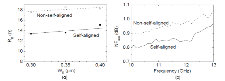
Figure 6. (a) Base Resistance vs. Emitter width WE for Self-aligned and Non-self-aligned HBT for an Emitter Length of 20 μm, (b) NF vs Frequency for a Low Noise Amplifier (LNA) for Identical Circuit Design and Identical Bias Conditions
Two figure of merits are generally used to benchmark high-frequency devices performance, the cut-off frequency f , defined as the frequency at which the small- T signal gain is unity, and the maximum frequency of oscillation f , defined as the frequency at which the max power gain is unity. These metrics, as it is known [50], are related to the transistor parameters, such as the forward transit time, sum of the delay times attributes to charge storage in different regions of the device, the emitter-base capacitance, the base-collector capacitance, the emitter series resistance, the collector resistance, and the collector current.
Scope of the scaling procedure is the achievement of ever-higher values of f and f in order to ensure T max adequate margin in emerging applications circuit design. Furthermore, obtaining ever-higher peak f (f ) is T max important because high values of these metrics can be traded-off in order to achieve better performance in terms of power consumption, breakdown voltage and circuit noise. As shown in Figure 7, that reports fT and fmax progression through multiple generation of IBM SiGe process [16], power saving can be achieved employing higher f (f ) SiGe technology although the circuit T max operating frequency is far lower, since for a given frequency the corresponding collector current decreases as the peak f increases.
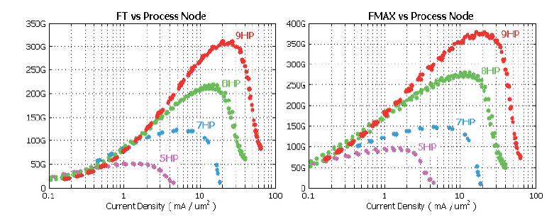
Figure 7. f and f Progression through Multiple Generations of IBM SiGe
Furthermore, for a given gain specification, making use of higher f transistors, the number of gain stages will reduce T resulting in improvements in terms of power consumption, circuit area, and total noise added by the circuit. Operating at lower collector currents with high f devices, T noise performance further enhances. Finally, f can be T traded off for high breakdown voltage using less aggressive collector doping profiles. Although each subsequent technology generation supports devices with higher f and f , it also improves the trade-off between T max speed and breakdown voltage, modulating the collector doping concentration. Objective of the vertical scaling is to reduce the forward transit time to increase f trying to T affect as little as possible on f performance.
Generally, vertical scaling is performed on three different directions.
The first concerns the Ge base profile. The high current gain resulting from the increase of Ge content in the base can be treated with a higher doping base profile that allows the aggressive reduction of the base width without encountering punch-through issues. Furthermore, increasing the slope of the Ge profile leads to high quasielectric field across the base. Both these expedients allow the reduction of the base transit time resulting in higher f . T Unfortunately, thinning the base layer leads to an increase of the base resistance which directly affects f .
The second strategy concerns the collector scaling. Increasing the collector doping results in a reduction of both collector transit time, due to the reduce of the B-C space charge, and the collector resistance. Two main issues arise from this strategy. Reducing the B-C spacecharge unavoidably leads to an increase of the B-C capacitance which in turn degrades f . Furthermore, as max previously discussed, increasing the collector doping leads to a lower breakdown voltage, factor to take into consideration in HBTs design.
Finally, the third strategy relates the emitter scaling. The reduction of the emitter transit time and the emitter series resistance can be achieved increasing the emitter doping. However, the upper limit for the simultaneous emitter and base scaling is imposed by tunnelling leakage currents phenomena, occurring when the doping concentration on the low doped side of the E-B -3 junction is greater than about 5×1018 cm [10]. As a result of the vertical scaling, improvements in base transit time and collector transit time, resulting in higher values of f , T are achieved at the expenses of an increase of both the base resistance and the B-C capacitance. Furthermore, the reduction of the annealing temperature improves f T but is detrimental to f since it degrades the base max resistance.
The trade-off between f and f is better illustrated in Figure 8(a) where is evident the competitive behaviour of the base and collector scaling [8], [58].
Objective of the lateral scaling is the decrease of the base resistance and the B-C capacitance in order to increase f . At the heart of the lateral scaling of SiGe HBTs is the max reduction of the emitter window width that leads to a decrease of the intrinsic C-B capacitance and the intrinsic E-B capacitance due to the reduction of the B-C and B-E junction areas. Furthermore, shortening the base resistive current path, the extrinsic base resistance also scales down. The reduction of polyemitter width, for a given window width, further reduces the extrinsic base resistance and the extrinsic E-B capacitance since it reduces the poly-emitter/poly-base overlap and brings the silicide closer to the intrinsic base. The main drawback associated to the reduction of emitter width is the increase of the emitter series resistance, due the laterally narrowed vertical current paths, as shown in Figure 8(b). Since the increase of the emitter resistance cannot be avoided it should be limited in order to ensure high f T values. This is done through an accurate scaling procedure aimed to balance the competitive effect of the reduction of both B-C and B-E capacitances and the increase of emitter resistance making possible the simultaneous improvement of f and f with decreasing T max the emitter width, as illustrated in Figure 8(a).
Recent improvements in SiGe HBT have made SiGe BiCMOS a mainstream technology for a large variety of commercial mm-wave integrated circuits in the automotive, communication and instrumentation sectors. Three main applications will drive SiGe HBT technology improvements in the next 15-20 years, mmwave
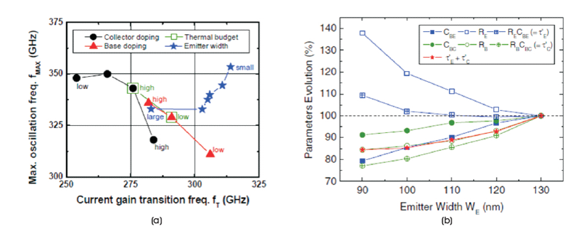
Figure 8. (a) f vs. f of Si/SiGe:C HBTs [58], (b) Evolution of the Si/SiGe:C HBT parameters with the emitter width [8]
In the latest edition ITRS [66] f and f are predicted to T max reach 780 GHz and 2 THz, respectively beyond the year 2030.
Moreover, TCAD simulations intended to predict benchmark circuits per formance across future technology nodes, indicate that PAs with 45% Power Added Efficiency (PAE), 7 dB gain, 10.6 dBm output power and TIAs with over 175 GHz bandwidth and less than 3dB NF will be achievable by the year 2030.
The attainment of these objectives raises at least two major issues. The first concerns the introduction of new scaling strategies in order to achieve highly doped regions with ever-higher Ge slopes, low contact resistances and sufficiently low process tolerance, essential features to obtain the predicted performance. Furthermore, the continuing decrease in HBT devices size and enhanced increase in current densities lead to concern about the impact of the temperature increase on device electrical characteristics.
On the other side, TCAD based simulations suggest that, despite, the advantages offered by strain channels, MOSFETs performance will saturate at an f about 600 GHz T and then degrade due the onset of evermore preponderant second order effects, as the gate length scales down from 10 nm to 5 nm. This behaviour is opposite to that followed by SiGe HBTs, where shrinking the emitter width from 66 nm to 22 nm, featured from the predicted N5 technology node, high-frequency performance continues to improve proportionally to the scaling factor. Since the significant SiGe HBTs progress over the last few years and the large room of improvements in scaling techniques, TCAD simulation results are quite encouraging for the development of mm-wave integrated systems, based on SiGe BiCMOS technology, aimed to address emerging applications requirements.
technology have been discussed using a circuit-oriented approach. Through an analysis of high-performance circuit blocks, such as PAs, LNAs, Oscillators, Mixers, and integrated transceivers recently realized, we could say that SiGe HBTs represent a milestone for the development of the analog and mixed signals of integrated systems suitable for emerging ultra-low-power, high-speed, and wide-bandwidth applications. Although today SiGe BiCMOS technology performance are sufficient for the development of ICs operating at frequencies up to 120 GHz, there is still a lot of work to be done in order to address emerging applications requirements. Furthermore TCADbased simulations of SiGe HBT devices, with f and f of T max 780 GHz and 2 THz, respectively, are very encouraging for the development of future SiGe ICs, planned by 2030.