[1]
This paper deals with the simulation of Cascaded Interleaved Buck Converter (IBC) with open source operation having low switching losses, less ripple and improved step-down conversion ratio, which is suitable for the application where the input voltage is high. A series of active switches with coupling capacitor are employed in the power circuit. This paper deals with Cuk, Sepic and Zeta converters. All active switches are only stressed with half of the input voltage before turning on or after turning off the proposed IBC. The capacitive discharging and switching losses can be reduced considerably to have higher efficiency, higher step-down conversion ratio, higher switching frequency and a smaller output ripple compared with a conventional IBC. The model of cascaded Interleaved buck converter system are presented.
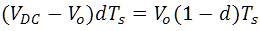
Interleaved Buck Converter has gained lots of concentration due to its simple and low control complexity in applications. where no isolation and high output current with low ripple are required. A Non isolated DC/DC converter or step-down DC/DC converter is shown in Figure 1. [13] When switch M is on for the duration of dTs, power is transferred from source to load and filter inductor L is charged. When switch M is off for a duration (1-d)Ts, the diode D becomes forward-biased and forms a conduction path for the filter inductor current. The voltage across the filter inductor is the reverse of the output voltage. By using this filter inductor volt-second balance rule is given below

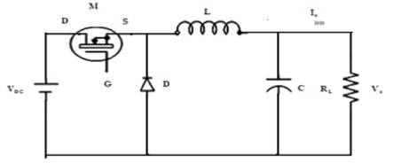
Figure 1. Step-down (Buck) converter
As observed from equation (1)&(2), the regulated output voltage (Vo ) is lower than the input voltage(VDC ). P.L.Wong, P.Yang and F.C.Lee (2001): C. Garcia, P. Zumel, A.D. Castro, and J.A. Cobos (2006): Y.C. Chuang(2010) emphasized that the Interleaved Buck Converter has got lots of attention due to its simple and low control complexity in applications where no isolation , step-down conversion ratio, and high output current with low ripple are required, but they could not able to reduce the ripple. [2]
In the conventional IBC all active switches suffer from input voltage, and hence, high-voltage devices rated above the input voltage should be used. High-voltage rated devices generally have poor characteristics such as high cost, high on-resistance, high forward voltage drop, severe reverse recovery, etc. Due to the hard switching condition, the cost becomes high and the efficiency becomes poor. For higher power density and for fast response, the converter operates at higher switching frequencies citied by. C.S. Moo,Y.J.Cinen, H.L.Cheng, and Y.C.Hiseh (2011) and also, the higher switching frequencies increase the switching losses associated with turn-on, turn-off, and reverse recovery which in turn reduce the efficiency.
To avoid the drawbacks of the conventional IBC, and to reduce the voltage stress of a buck converter, different types of IBCs have been presented by the researchers. In J.P. Rodrigues, S.A. Mussa, M.L. Heldwein and A.J. Perin (2009): X. Du and H.M. Tai (2011) [7]-[9] three-level buck converters are introduced and the voltage stress is half of the input voltage in the converters but anyway the number of components required for the IBC is more. In Y.M.Chen, S.Y.Teseng, C.T.Tsai, and T.F.Wu, (2004) [11], an IBC with active clamp circuits are introduced[12]. In the converter, all active switches are turned ON with zero voltage switching by which a high step-down conversion ratio can be obtained and the voltage stress across the freewheeling diodes can be reduced [8]. The cost is increased for the mentioned advantages, by the addition of passive and active components. J.Y.Lee, Y.S.Jeong, and B.M.Han (2011) cited IBC with two winding coupled inductors when introduced which operates at Continuous Conduction Mode (CCM), the current stress is lower than that of discontinuous conduction mode IBC.
In this paper, a novel cascaded IBC, which is suitable for the applications where the input voltage is high and the operating duty is below 50%, is proposed. In the conventional IBC, the active switches are connected in parallel but in this converter two active switches are connected in series and a coupling capacitor is employed in the power path. The two active switches are driven with a phase shift angle of 180° and the output voltage is regulated by adjusting the duty cycle at a fixed switching frequency. The proposed IBC operates at CCM and the current stress is low. The voltage stress across all active switches before turn-on or after turn-off. during the steady state is half of the input voltage.
Hence, the capacitance discharging and switching losses are reduced. The voltage stress on the freewheeling diode, conversion ratio and output current ripple are lower than that of the existing converter.
The circuit operations, their relevant analysis results, and the conclusion for the proposed system is given in the forth coming sections.
Figure 2. shows the circuit diagram of the open loop Interleaved Buck Converter IBC with C filter. The structure is similar to a conventional IBC. The active switches are connected in parallel but in this converter, two active switches are connected in series and a coupling capacitor is employed in the power path. The two active switches M and M are driven with phase shift angle of 1 2 180°. Figure 2 (a). shows the circuit diagram of the proposed interleaved buck converter with cascaded filter. When the cascaded filter was used in the circuit the output power increased and the ripple is very much reduced. This has been discussed in the forth coming topics.
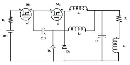
Figure 2. Circuit diagram of IBC
Figure 2 (a). Circuit diagram of Proposed cascaded IBC
Each switching period is divided into four modes, For the operation of this converter, some assumptions are made as follows:
a. The output capacitor Co and coupling capacitor CB should be large, as it acts as the voltage source.
b. The L1 and L2 inductors are equal.
c. All MOSFETs are ideal
Figure 2. shows the Circuit diagram of the Proposed cascaded IBC
The four modes of operations are explained below,
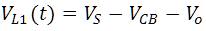
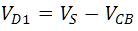
In this mode, M1 is turned ON, the current of L1 , iL1 (t), flows through M1 , CB , and L1 and the voltage of the coupling capacitor VCB is charged. The current of L1 , iL2 (t), freewheels through D2 .During this mode, the voltage across L1 , VL1 (t),is the difference of the input voltage Vs , voltage of coupling capacitor VCB , and the output voltage Vo is positive. The voltage across L2 , VL2(t),is negative output voltage Vo . Hence, iL1 (t) and iL2 (t), increases and decreases linearly from the initial value.
The voltages are expressed as,
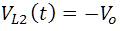
In this mode, M1 is turned OFF at t1 . Then, iL1 (t) and iL2 (t) freewheel through D1 and D2, VL1 (t) and VL2 (t) becomes negative Vo , and hence iL1 (t) and iL2 (t) decrease linearly The voltages are expressed as

In this mode, M2 is turned ON, D2 is turned OFF. At this time, iL1(t) freewheels through D1 ,CB , M2 and L2 . During this mode, VCB is discharged, VL2 (t) = VCB – Vo and is positive, VL1 (t)= -Vo , iL2(t) and iL1 (t) increases and decreases linearly.
In this mode, M2 is turned OFF and its operation is same as the mode 2.
The simulation is done using Matlab simulink and the results are presented here. The Open Loop Cascaded IBC is shown in Figure 3. Input voltage of 220 V DC for Open Loop Circuit with cascaded filter is shown in Figure 3(a), Output voltage of 48 V for Open Loop Circuit with cascaded filter is shown in Figure 3(b). Output voltage ripple for Open Loop Circuit is shown in Figure 3(c). Figure 3(d). shows the Open Loop Cascaded Buck Interleaved Converter Output Power. The ripple produced by the Interleaved buck converter with cascaded filter was 0.0015 for output power of 115W.
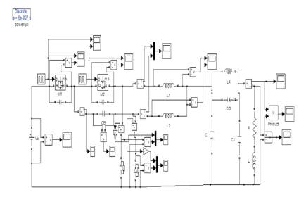
Figure 3. Open Loop Cascaded Buck Interleaved Converter Circuit with cascaded filter.
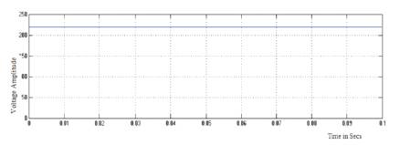
Figure 3(a). Input voltage for Open Loop Circuit.
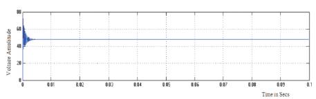
Figure 3(b).Output voltage for Open Loop Circuit.
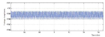
Figure 3(c).Outputt voltage ripple for Open Loop Circuit.
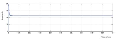
Figure 3(d).Open Loop Cascaded Buck Interleaved Converter Output Power..
The Cascaded Interleaved Buck Converter Open Loop is modeled and simulated using Matlab simulink. The results of simulation are presented in this paper. This converter has advantages like less ripple, improved step down ratio and reduced losses. The results of this modified circuit are also presented. The variation of output 48V DC with the variation with the input voltage 220V DC with cascaded filter was simulated. The simulation results are in line with the predictions.