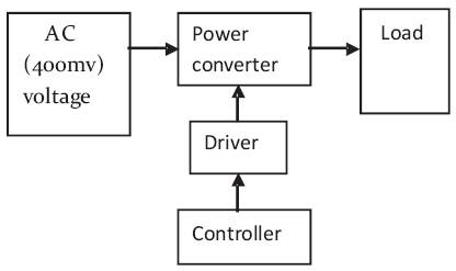
Figure 1. Proposed Block Diagram of AC-DC Converter
In this paper, an ac/dc converter is presented that can boost very low ac voltages to a higher dc voltage. The converter is based on a new hybrid form of boost converter and a buck boost converter and it is suitable for power harvesting applications too. The measured prototype can supply 3.3V by converting an input voltage of 400mV delivered by an electromagnetic micro generator. Detailed analysis of converter is carried out and based on that control schemes are proposed to operate the converter.
Energy from ambient sources are a viable alternative for supplying power to a variety of applications. Ambient energy is energy that is in the environment of the system and is not stored explicitly. Portable systems that depend on batteries have a limited operating life and can fail at inconvenient times, while a circuit powered by ambient sources has a potentially infinite life time. Inertial miicrogenerators which harvest mechanical energy from ambient vibrations are currently the focus of many research groups. Electromagnetic microgenerators among the various inertial generators [15] (piezoelectric, electrostatic and electromagnetic) have the highest energy density and it is considered for further study.
In electromagnetic microgenerators, small amplitude ambient mechanical vibrations are amplified into larger amplitude translational movements and the mechanical energy of the motion is converted to electrical energy by electromagnetic coupling(1),(5)-(13). The output thus produced is of ac type with very low magnitude. In order to use this voltage as a supply source to electronic loads, it has to be converted into dc and must be stepped up. This requires two stages of conversion: first, ac should be rectified to dc and then it must be stepped up to the necessary dc voltage. For very low voltage as in microgenerators, rectification is not feasible by the use of conventional diodes. Even if the diode bridge rectification is possible, the forward voltage drop in diodes will cause a large amount of losses and makes the power conversion inefficient.
In this paper a new method is introduced in which low voltage ac is stepped up into dc in a single stage. A boost and a buck boost converter are connected in parallel to get the desired output. The block diagram is shown in Figure 1.
Figure 1. Proposed Block Diagram of AC-DC Converter
In the above block diagram, the ac supply is from a electromagnetic microgenerator supplying a peak voltage of 400mV. The power converter is used to convert the ac signal to dc signal and to step up the dc. This block consist of a boost converter connected in parallel to a buck boost converter. The microcontroller is used to generate the PWM pulses for triggering the switches and the driver circuit amplifies the generated PWM pulses.
The proposed circuit diagram is shown in Figure 2.
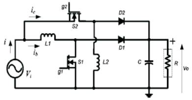
Figure 2. Circuit Diagram of AC-DC Converter
It consist of a boost converter connected in parallel to a buck boost converter. Inductor L1, switch S1,and diode D1 together form the boost converter. Inductor L2, switch S2, diode D2 belong to buck boost converter .The output capacitor C is charged by the boost converter in the positive half cycle, and by the buck boost converter in the negative half cycle. The operation of the circuit is based on the switching ON and switching OFF of both the above mentioned switches. It can be noted that the input current and inductor S1 are same during both switching ON and OFF of the switch S1. But in case of buck boost converter the input current becomes zero when S2 is OFF. In order to convert and step up ac to dc, the revere polarity of buck boost converter is used to boost the voltage of negative half cycle of microgenerator to positive dc voltage.
The operation of circuit can be broadly be divided into 4 different modes. Mode 1 and 2 belong to the positive half cycle when boost converter operates. Modes 3 and 4 belong to the negative half cycle when buck boost converter operates.
During mode 1, S1 will be ON. The ac source voltage delivers power to the inductor L1, and it stores energy. In this mode diode D1 is reverse biased. The precharged capacitor delivers power to the load at this mode. At mode 2, S1 will be OFF. Now D1 becomes forward biased. The supply along with the energy stored in the inductor (during mode1) delivers power to the load and charges the capacitor.
During mode 3, S2 will be ON and inductor stores energy. At mode 4, when S2 is OFF, energy in L2 feeds the capacitor and the load. In a switching cycle the energy transferred to the output by a buck boost converter is equal to the energy stored in the inductor L2, where as in the boost converter, the energy transferred to the output is more than the energy stored in the inductor. The proposed converter is operated under Discontinuous Mode of Operation (DCM). This reduces the switch turn ON and turn OFF losses. The DCM operation also reduces the diode reverse recovery losses of the boost and buck–boost converter diodes. Furthermore, the DCM operation enables easy implementation of the control scheme. It can be noted that under constant duty cycle DCM operation, the input current is proportional to the input voltage at every switching cycle; therefore, the overall input current will be in-phase with microgenerator output voltage.
Consider any kth switching cycle of boost and buck boost converter as shown in Figure 3 [2].Ts is the time period of switching cycle, Db is the duty cycle of boost converter, dfTs is the boost inductor current fall time (diode D1 conduction time).
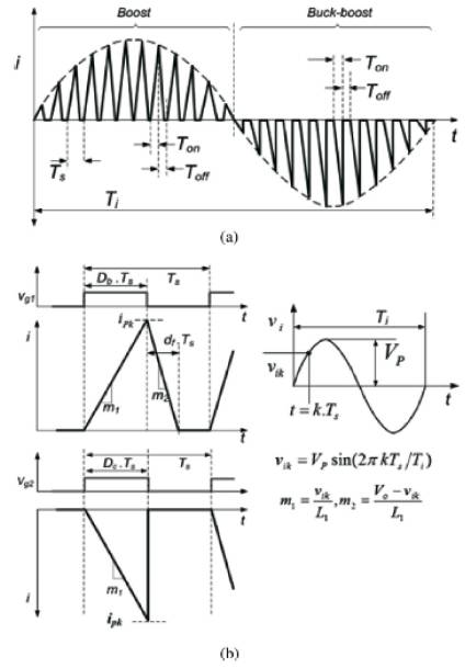
Figure 3 (a) Input Current Waveform of Converter (b)Input Currents, Gate Drive Signals and Input Voltage During a Switching Cycle of Boost and Buck Boost Converter
Dc is the duty cycle of buck boost converter, Vi is the input voltage of generator with amplitude Vp and Vo is the converter output voltage
Assume switching time period (Ts) of converter as much smaller than the time period of output ac cycle (Ti)
Ts< < Ti
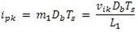
Peak value of inductor current can be obtained as
Where
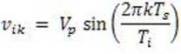
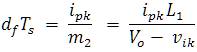
After the boost converter switch is turned OFF, the current in the inductor starts to fall (see Figure 3). The slope (m2) of this current is decided by the voltage across the inductor. In a kth switching cycle, the voltage across the inductor during the inductor current fall time is: Vo − vik . Therefore, the inductor current fall time can be found as in
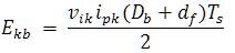
During this kth switching cycle, the total energy (EKB) transferred from the input of the boost converter can be obtained as in (3)
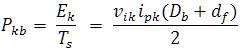
The average power supplied in the boost switching cycle is
The number of switching cycles during the time period of one input ac cycle is defined as N = Ti/Ts . In the proposed power electronics converter topology, the boost converter is operated for the half time period of the input ac cycle (Ti /2). The average input power Pib of the boost converter over this half cycle time period can be obtained as in (5)
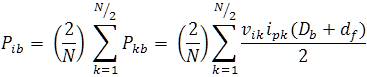
For large N, the discrete function in (5) can be treated as a continuous function. The average input power of the boost converter Pib (5) can be obtained by integrating the term in the summation over the half cycle (Ti/2) period of the input ac voltage and then taking its mean value. The average power of the boost converter expressed in the integration form can be obtained as in (6)
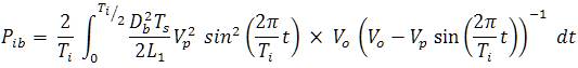
where the microgenerator input voltage is defined as: νi = Vp sin(2πt/T)[2].
Simplifying (6), the average input power for the boost converter Pib is found to be as follows
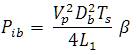
Where
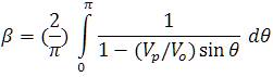
and,

It can be noted that in (7), β is constant for fixed values of Vp and Vo. Also, it is seen that for large switching frequency of the converter, the average power is independent of the microgenerator output voltage frequency.
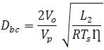
In steady state, the average input power of the converter is equal to the sum of the average output power and the various converter losses. Hence, by defining the converter efficiency as η for a load resistance R, the input power and the output power can be balanced as in (8)
From (8), the duty cycle of the boost converter (Db ) can be obtained as
Further, consider the operation of the buck–boost converter; in this case the input power is supplied only during the ON period of the switch S2 (see Figure 3). During the OFF period of the switch S2 , the input current is zero [see Figure 3(a)]. Hence, for any kth switching cycle, the average power supplied by the buck–boost converter PKC can be obtained as
Applying similar approach, used earlier for the boost converter, the average power can be expressed in the integration form as
The duty cycle Dc can be obtained as in (12)
For a given microgenerator and a load ,the input and output voltages are specified. The voltage rating of MOSFETS are decided by the output voltage of the converter. Current rating of MOSFET has to be designed by the designer. MOSFET carries maximum current at peak input voltage. Maximum current Imax is given as in (13)
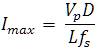
Here fs is the switching frequency of converter, L is the inductance of both boost and buck boost converter, and D is the duty cycle of converter (Db=Dc=D). Another equation used to find maximum current is
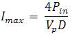
Figure 4 shows relations graph between inductor current and duty cycle. Also, the graph between inductance and duty cycle is shown.
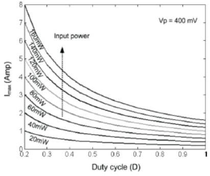
Figure 4. Design Graphs. Duty Ratio Versus Maximum Input Current
Using the Figure 4, MOSFET current values and duty cycle can be selected. With these values in the given equation, the inductor value, L and switching frequency fs can be found out. Figure 5 shows the relation between the value of inductor (L) and the duty cycle over a range of frequencies. Using these charts and equations, the initial values of the key components of the converter can be decided. The duty cycle and the frequency of the converter can be appropriately selected to choose the desired value of the inductor. In this study, the proposed converter is designed to supply about 55mW of power to the load.
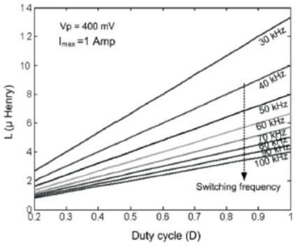
Figure 5. Design Graph Between Inductance and Duty Cycle
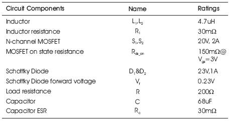
Table 1. Circuit Components of the Converter
The controller and the MOSFET driver circuit of converter are required to be self starting [2], and they should be powered by energy harvesting system. An auxiliary self starting circuit comprising of a battery and schottky diode is proposed to power the controller and driver at the beginning when the converter starts up (Figure 6). The battery nominal voltage Vb should be less than the target output voltage Vo minus the forward voltage drop of a diode Vf ,and it should be above the minimum voltage requirements of the controller and driver circuits [4].
Here the target output voltage Vo = 3.3 V and forward voltage drop of the diodes Vf = 0.22 V. A battery with nominal voltage Vb = 3 V is selected for the self-starting. At the beginning of the converter operation, when the output voltage Vo is not available, the controller and the driver circuit will be powered by the battery through the Schottky diode Db. This will allow the converter to charge the output capacitor to the reference voltage. In steady state, when the output voltage has reached the value 3.3 V, the diode Db would be reverse biased, therefore, the battery will not be powering the controller and the driver. At this time, they will be powered from the converter output through the diode Da. During this condition, the battery will remain under floating condition. It can be noted that only a very small amount of energy is taken from the battery for the startup of the energy harvesting system. Furthermore, the used energy of the battery can be replenished by recharging it from the output of converter through the diode Dc. Therefore, the entire amount of energy used for the converter operation, including the energy used during its starting, is harvested from the ambience.
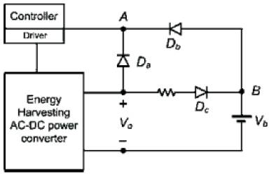
Figure 6. Auxilliary Self Starting Circuit Using a Battery
A resonance-based electromagnetic microgenerator, producing 400 mV peak sinusoidal output voltage, with 100-Hz frequency is considered in this study for verification of the proposed converter topology. The open loop and closed-loop simulation of the converter is carried out. The reference output voltage (Vref) is considered to be 3.3 V and the switching frequency of the converter is selected to be 50kHz. The energy-harvesting converter is designed for supplying power to a 200-Ω load resistance, hence, supplying about 55 mW of output power.
Simulation of open loop and closed loop circuit has been done. Figure 7(a) shows the simulation diagram of an open loop system. Figure 7(b) shows output voltage waveform of open loop ciruit. Figure 8 shows the input voltage, boost input current, buck boost input current ,source current and the switching pattern of both boost and buck boost converters (S1 and S2 respectively). In open loop a maximum of 2.86V is obtained as shown in simulation.
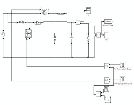
Figure 7(a). Simulation Diagram of Open Loop Circuit
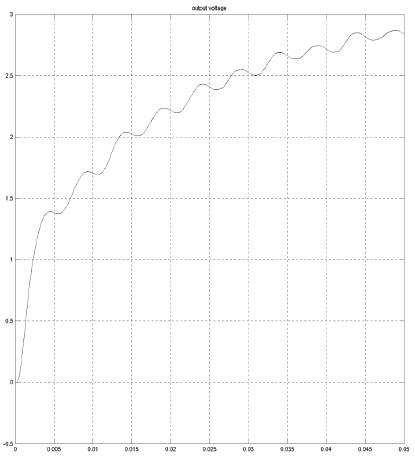
Figure 7(b). Output Voltage Waveform of Open Loop
In Figure 8, the input voltage of microgenerator is shown as a sine wave with peak amplitude of 400mv. The switching ON an OFF of switches in the boost and buck boost converter gives the current through the inductor. The switching pattern of both converters is also shown. During the positive half cycle only the boost converter is switched. In the negative half cycle, the buck boost converter is switched as shown in the Figure 8.
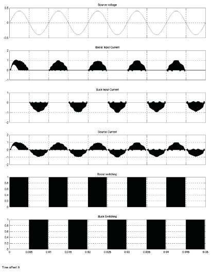
Figure 8. Input Voltage, Input Current to Boost Converter, Buck Boost Converter, Source Current, Switching of Boost and Buck Boost Converter
Simulation is carried out in MATLAB 7.9.0 (R2009b) version. Figure 9 shows the simulation diagram of a closed loop control. Here we are using PI controller. Figure 10 shows the output voltage waveform under closed loop. It is clear from the above two graphs that under closed loop control a better output close to the desired dc voltage of about 3.267 is obtained. While in open loop a value of 2.86V is obtained.
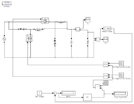
Figure 9. Simulation Diagram of PI Controller
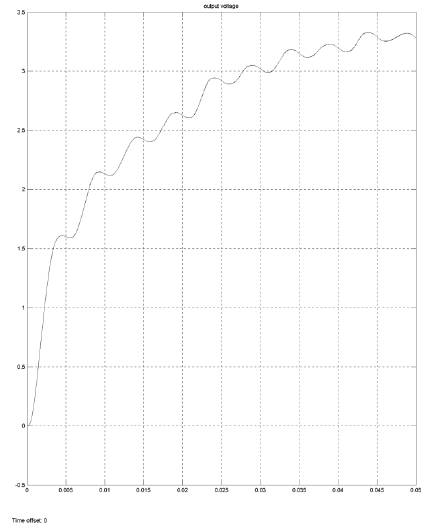
Figure 10. Output of Converter with PI Control
Further, the simulation is also done under fuzzy logic control as shown in Figure 11. From the output voltage (Figure 11,(b)), it can be seen that it gives an output of about 3.3V. In spite of its practical success, fuzzy logic has been criticized for its limitations, such as the lack of a formal design methodology and the difficulty in predicting stability and robustness of FL controlled systems.
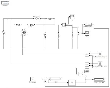
Figure 11(a). Simulation Diagram
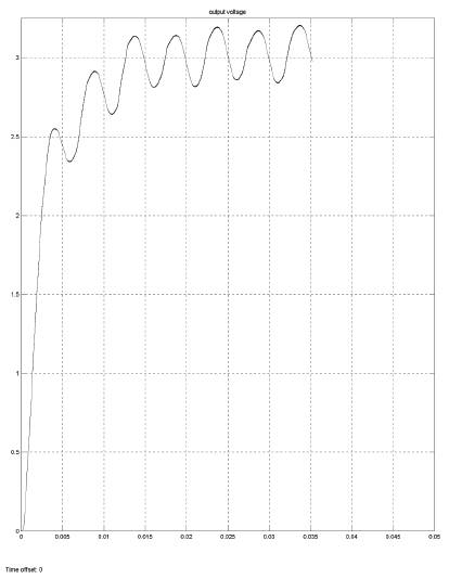
Figure 11(b). Output of Converter with Fuzzy Control
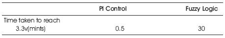
Table 2. Comparison of PI And Fuzzy Control
The efficiency of the mentioned converter is about 61%.This value can be further increased by replacing the diodes by MOSFETs. Also, with the use of larger MOSFETs with lower ON state resistance, the efficiency can be further improved. Another improvement could be the design of an auxiliary circuit that stores charge when the load is removed. With proper design of the conductor and magnetic components, the converter performance can further be enhanced. [14]
A direct ac-to-dc low voltage energy harvesting converter is proposed in this paper. Detailed analysis of the converter for direct ac -to-dc power conversion is carried out and the relations between various converter circuit parameters and control parameters are obtained. Design guidelines are presented for selecting values of the key components and control parameters of the converter. A self-startup circuit, using a battery only during the beginning of the converter operation, is proposed for the energy-harvesting converter. Operation and the implementation of the self-startup circuit and the control circuit of the converter are presented in detail.
Output of the converter in open loop, and closed loop using PI controller and fuzzy logic control are presented (Table 2). Better results are obtained in closed loop circuit. An output of 3.267V is obtained from a 400mV ac supply using the proposed system giving an efficiency of about 61%.