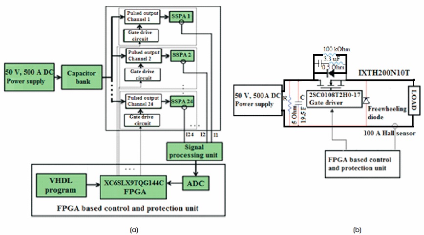
Figure 1. (a) Schematic of Pulsed Power Supply with 24 Numbers of 50 V, 80 A Pulsed Output Channels, (b) Schematic of One 50 V, 80 A Pulsed Output Channel
This article presents an FPGA based control and protection unit employing Xilinx make Spartan-6 XC6SLX9TQG144C FPGA for driving a multichannel pulsed power supply of pulsed solid state RF amplifiers. The control unit generates synchronized drive pulses for driving 24 units of 50 V, 80 A pulsed output channels of the multichannel pulsed power supply. The pulse width and frequency of drive pulses are settable from 100 μs to 2.5 ms and from 1 Hz to 50 Hz respectively. Over-current protection of output channels is implemented through its protection unit. The FPGA has been programmed in VHDL for pulse generation, control of pulse parameters and over current protection of pulsed output channels. The schematics, simulation results and RTL schemes are presented in this paper. This control and protection unit is integrated with 24 numbers of 50 V, 80 A pulsed output channels which are simultaneously tested up to 80 A peak current and experimental results are also presented in this paper. The rise time and fall time of output pulse are observed as < 20 μs and voltage droop is observed as < 0.5%. Typical jitter among output pulses of different pulsed output channels is observed as 60 ns.
A pulsed solid state RF amplifier based RF source at 325 MHz is developed for providing RF power to different particle accelerators, wherein, the RF power is generated by combining the outputs of several 1.5 kW, 325 MHz pulsed solid state RF power amplifiers (SSPA). Both DC and pulsed power supply can be employed for biasing pulsed SSPA but pulsed power supply offers many advantages over its DC counterpart. The ratings of switchgear elements like contractor, fuse and MCB of DC power supplies are decided by keeping their continuous full load operation in view ( Kumrawat et al., 2013; Larsen et al., 2016). If a DC power supply is employed for pulsed application, the r.m.s. input current drawn by the power supply will be much less and switch gear elements used in it will be ineffective. Thus, these switch gear elements will not be able to protect the semiconductor devices and other sensitive elements of DC power supply. When RF drive pulse is applied to a pulsed SSPA biased by DC power supply, initial transients of high amplitude appear in RF output pulse for longer time duration, whereas these transients are less severe with pulsed power supply. If pulsed SSPA is biased by DC power supply, it continues to draw bias current during OFF period of RF pulse which results in additional power loss and reduces the efficiency of overall RF system ( Deo et al., 2018). But if pulsed SSPA is biased by pulsed power supply, the efficiency of overall system improves.
Each 1.5 kW RF amplifier draws up to 80 A peak current so a multichannel pulsed power supply having 24 numbers of 50 V, 80 A pulsed output channels has been developed to bias 24 numbers of pulsed SSPAs. The drive pulses of variable pulse width and frequency can be generated by analog or digital controller. As digital signals are more adjustable, less affected by noise, more secure, have higher transmission rate and can be processed easily by processing tools as compared to analog signals, so digital controllers are preferred over analog controllers. Traditionally, there are three hardware control platforms available for implementing digital controllers: Digital Signal Processors (DSPs), Field Programmable Gate Arrays (FPGA), and Application Specific Integrated Circuits (ASICs). FPGAbased applications include many benefits of DSPs and ASICs ( Bianchi & De Munari, 2020; MacLean, 2005; Monmasson et al., 2011). FPGA is advantageous in terms of higher number of logic gates, operating speed and power consumption ( Maerani et al., 2018; Mekala & Fan 2011; Roy et al., 2019) whereas with high data rates, a DSP may suffer from scanning, processing and extracting data without loss. ASICs are custom made for specific requirements, however, they lack flexibility for changes meaning they are having low re-configurability and are also difficult to test and debug ( Bouldin et al., 2004; Chowdhury et al., 2008). Again, as the pulsed RF outputs of different SSPAs need to be in proper synchronism for generating necessary output RF power. The output pulses of different pulsed output channels biasing these SSPAs also need to be properly synchronized with least possible jitter among them. The synchronization among drive pulses of different pulsed output channels is easily achieved with high speed FPGA ( Herbordt et al., 2007; Janky & Varga, 2018; Li et al., 2018). FPGAs also implement faster and parallel signal processing ( Torquato & Fernandes, 2019). So based on the advantages offered by FPGAs, an FPGA based control and protection unit is developed to generate synchronized gate drive signals for driving 24 numbers of 50 V, 80 A pulsed output channels. Here, the pulse width of output pulse is settable from 100 μs to 2.5 ms and frequency is settable from 1 Hz to 50 Hz.
The pulsed power supply contains 24 numbers of 50 V, 80 A pulsed output channels to bias 24 numbers of pulsed solid state RF amplifiers. It is developed by charging a capacitor bank with the help of a constant current controlled voltage (CCCV) DC power supply and then discharging its stored energy with the help of MOSFET switches employed in pulsed output channels to generate output pulses (Tripathi et al., 2018). The 50 V, 80 A pulsed output channel contains an IXYS make 100 V, 200 A, MOSFET switch (IXTH200N10T), a Power Integration make gate driver (2SC0108T2H0-17) and an IXYS make freewheeling fast recovery diode (DPG60C200HB). The schematic of pulsed power supply containing 24 numbers of 50 V, 80 A pulsed output channels along with FPGA based control and protection unit is shown in Figure 1(a) and the schematic of a 50 V, 80 A pulsed output channel is given in Figure 1(b). The load currents of all pulsed output channels are sensed through hall sensors and given to signal processing unit. The signal processing unit takes the voltage output signals from sense resistors of hall sensors and filter out high frequency components. The output of signal processing unit is given to control and protection unit for over current protection purpose. Total capacitance requirement of pulsed power supply (C) is given as, C = I x Δt/ΔV, where, I = total peak current, ΔV = permissible voltage droop and Δt = pulse ON time. Now, putting I = 24 x 80 = 1920 A, ΔV = 0.5% of 50 V = 0.25 V and Δt = 2.5 ms in this equation, required capacitance is found as C =19.2 F. To reduce voltage droop below 0.5%, a capacitor bank of slightly higher value, i.e. 19.5 F, is formed by paralleling 888 numbers of 100 V, 22000 μF electrolytic capacitors. Charge lost from this capacitor bank during pulse ON time is, ΔQ = I x Δt = 1920 A x 2.5 ms = 4.8 C. This lost charge must be replenished in 17.5 ms, hence the output current requirement from DC power supply is, I = ΔQ / Δt = 4.8/ (17.5 x 10⁻³) = 274 A. So, a modular hot swappable 50 V, 500 A, CCCV DC power supply having 5 numbers of 50 V, 100 A DC power modules is used for charging this capacitor bank in slow start mode. During operation, 2 numbers of these power modules remain active redundant which helps in increasing the reliability of this modular power supply ( Badapanda et al., 2015).
Figure 1. (a) Schematic of Pulsed Power Supply with 24 Numbers of 50 V, 80 A Pulsed Output Channels, (b) Schematic of One 50 V, 80 A Pulsed Output Channel
The drive pulses required for operating pulsed output channels are generated by FPGA based control and protection unit. As the drive signal from FPGA board is a 3.3 V signal, so to convert it into 15 V signal, a signal translator unit is used, which is shown in Figure 2. In signal translator, a high accuracy, low drift instrumentation amplifier AD 620 is used which requires only one external resistor Rg for setting the gain of this stage. The output of signal translator is given to gate driver which generates +15 V/-8 V gate drive signal for driving MOSFET switch of pulsed output channels. The capacitor bank is formed by connecting capacitors through copper strips in place of copper cables and all the connections from capacitor bank to MOSFET switch and dummy resistive load in pulsed output channels have been done using litz wires of minimum possible length to reduce inductances of power circuit. In addition, suitable RC snubber components are employed across MOSFET switch. These measures help in reducing the over voltage stress across MOSFET switch during its turn OFF operation. Reduced inductances also help in minimizing rise time and fall time of output pulse. The photograph of fabricated pulsed power supply with 24 numbers of 50 V, 80 A pulsed output channels is shown in Figure 3.
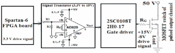
Figure 2. Signal Translator Unit
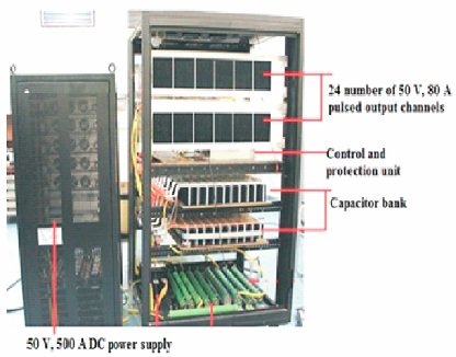
Figure 3. Photograph of Pulsed Power Supply with 24 Number of 50 V, 80 A Pulsed Output Channels
The interconnecting cable lengths of all pulsed output channels are kept same to maintain synchronism among their output pulses.
The control and protection unit of this pulsed power supply employs a Xilinx make XC6SLX9TQG144C FPGA embedded in a Spartan-6 FPGA development board. The block diagram of this FPGA board is shown in Figure 4. This FPGA development board contains a 50 MHz clock, 8 MB FLASH memory, 12 bit ADC, 20 pin expansion connector, LCD interface, 7 segment display and a RESET switch among others. XC6SLX9TQG144C is 144 pin logic optimized FPGA with 102 input outputs (IOs), 9152 logic cells and 18 KB RAM blocks. This FPGA can be configured in two ways: one by using USB JTAG using Xilinx software and other by FLASH memory. Configuration of FPGA through JTAG gets erased with removal of power supply of FPGA board or by pressing reset button. So FPGA is first programmed by USB JTAG to verify programming and then the program is burnt into FLASH memory.
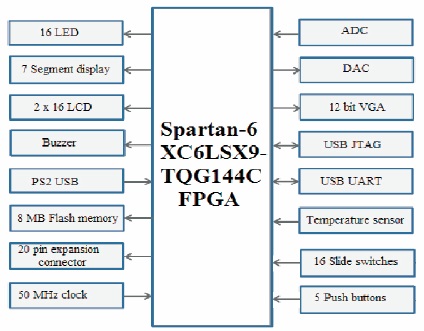
Figure 4. Block Diagram of Spartan-6 FPGA Development Board
The XC6SLX9TQG144C FPGA used in this Spartan-6 FPGA development board has been programmed in VHDL (Very high speed integrated circuit Hardware Description Language) programming language using Xilinx ISE 14.7 project navigator for pulse generation, over current protection and external control of pulse parameters (Xilinx, 2011).
The FPGA board has been programmed to generate drive pulses of maximum pulse width of 2.5 ms and maximum frequency of 50 Hz (corresponding to 20 ms time period). In VHDL program, an external loop is run for 20 ms duration, which repeats afterwards. Inside this loop, an inner loop is run for 2.5 ms for which the pulse output is high (or digital value “1”) and for the rest of 17.5 ms, output is “0”. As the clock frequency of Spartan-6 FPGA development board is 50 MHz corresponding to 20 ns clock period, hence for duration of 20 ms, FPGA clock has to be repeated for 20 ms/20 ns = 1000000 times. Value 1000000 corresponds to “11110100001001000000” in binary format. Similarly, for a duration of 2.5 ms, clock is repeated for 2.5 ms / 20 ns = 125000 times = “11110100001001000” in binary format.
For VHDL programming, a PRESCALER vector of std_logic variable of 20 bit length is defined (SIGNAL PRESCALER: STD_LOGIC_VECTOR (19 DOWNTO 0)). The binary value of 2.5 ms, i.e. 125000 is written as “00011110100001001000” in 20-bit format. The pulse output variable “pulseout” is defined as output std_logic variable and a local temporary variable “pulseout_temp” is also defined. The value stored in “pulseout_temp” variable is returned to “pulseout” variable. Variable "pulseout" is mapped to any particular IO pin of FPGA board through definition in user constraint file (UCF). The loop is run in behavioral modeling as follows,
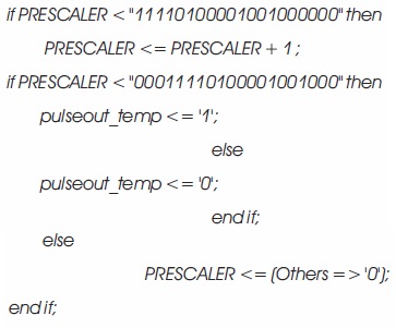
The schematic of VHDL program for single pulse generation by Xilinx ISE 14.7 software is presented in Figure 5. This schematic presents the various input and output signals of VHDL program which are defined as input (IN std_logic) and output (OUT std_logic) variables. The simulation waveform obtained by the VHDL program for single pulse generation is presented in Figure 6. It is clear from this simulation result that a pulse of 2.5 ms pulse width and 20 ms time period (50 Hz frequency) is generated by this VHDL program. The vector PRESCALER starts from "0000000 0000000000000" and keeps incrementing by 1 up to 20 ms time period ("11110100001001000000") and then repeats itself.

Figure 5. Schematic of Single Pulse Generation
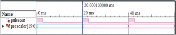
Figure 6. Simulation Waveform of Single Pulse Generation Program
Register transfer level (RTL) scheme is a graphical representation of the VHDL coded design in which standard combinatorial logic is mapped into logic gates. This scheme is represented in terms of adders, multipliers and registers. The RTL scheme of single pulse generation is presented in Figure 7.
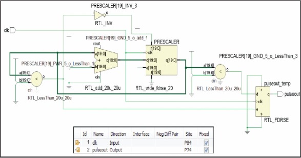
Figure 7. RTL Scheme of Single Pulse Generation Program
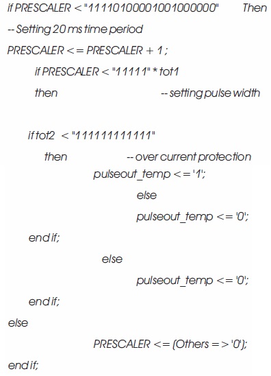
The FPGA based control and protection unit also sets the pulse parameters (pulse width and frequency) from external potentiometer and implements the over current protection of pulsed output channels along with drive pulse generation. The inbuilt ADC of Spartan-6 FPGA development board is utilized for these purposes. For setting the pulse width from an external potentiometer, the potentiometer output is given to one channel of ADC (setting of frequency from external potentiometer is similar to setting pulse width so is not presented here). For over current protection, the load current of one particular pulse output channel, taken by SSPA load, is sensed through hall sensor and given to another channel of inbuilt ADC after suitable signal processing. The program selects two ADC input channels, one for sensing potentiometer signal for setting pulse width and other for sensing output current of pulsed output channel. Corresponding analog values are converted to digital formats by ADC and are stored in two different temporary vectors “tot1” (for potentiometer signal) and “tot2” (for output current signal). Temporary vectors “tot1” and “tot2” are defined as std_logic vector of length 12 (variable tot: std_logic_vector (11 downto 0)) and initialized to “000000000000".
For including ADC in VHDL program, clock signal of FPGA board, “clk” and data input signal of ADC, “din” are defined as input std_logic variables. Signals serial clock “sck”, chip select “cs” and data output “do” of ADC and pulse output signal “pulseout” are defined as output std_logic variables. Again, a PRESCALER vector of std_logic variable of 20 bit length is defined (SIGNAL PRESCALER: STD_LOGIC_VECTOR (19 DOWNTO 0)). A local variable “pulseout_temp” is also declared.
It is established from pulse generation section that the clock is repeated for 125000 times (“1111010000 1001000” in binary) for generating 2.5 ms pulse. As the full scale value of 12 bit ADC is 212 -1 = 4095 so the value obtained by ADC converter (tot1) is multiplied with 125000/4095 = 30.525 ~ 31(binary value “11111”) to return 2.5 ms pulse width. The numerical value 31 is selected for multiplication to avoid floating point numbers. So in this way, desired pulse width can be set by varying potentiometer settings. Again, as the maximum analog value that can be given to any ADC channel of this FPGA board is 3.3 V, so 3.3 V is equated with the full scale value of “tot2” (= “111111111111”) and is assigned as the over current limit. If the over current limit for over current protection is chosen as 100 A, it must correspond to 3.3 V (i.e. 100 A = 3.3 V) and the current sensed by hall sensor is scaled accordingly.
The combined program of pulse generation, setting pulse width and over current protection runs three loops. The first loop sets the 50 Hz frequency (20 ms time period) which is already explained in pulse generation section. The second loop sets the pulse width. In this loop, the value of PRESCALER is compared with 11111" * tot1 and if the value of PRESCALER is less than “11111" * tot1”, the third loop is proceeded. The third loop implements over current protection. If the digital value of output current signal of any pulsed output channel “tot2” < “111111111111”, the local variable “pulseout_temp” is made high (i.e., “1”) or else “pulseout_temp” is 0. The value stored in “pulseout_temp” variable is returned to “pulseout” variable. Variable "pulseout" is mapped to any particular IO pin of FPGA board through definition in the UCF file. Thus, in case of over current of any pulsed output channel, the control and protection unit blocks the drive signal of that particular output channel. The combined program is run in behavioral modeling as follows,
The schematics of combined VHDL program for pulse generation, setting pulse width from external potentio meter and over current protection by Xilinx ISE 14.7 software is presented in Figure 8. The simulation waveform obtained by the combined program is shown in Figure 9. This simulation result shows that a pulse of 2.5 ms pulse width and 20 ms time period is generated. The vector PRESCALER again starts from 0 and keeps incrementing up to 20 ms time period and then repeats itself. In this waveform, the values of ADC parameters like "sck", "cs", "din" and "do" are as per the definition in VHDL program.

Figure 8. Schematic of Combined Program for Pulse Generation, Setting Pulse Width from External Potentiometer and Over Current Protection
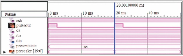
Figure 9. Simulation Waveform of Combined Program for Pulse Generation, Setting Pulse Width from External Potentiometer and Over Current Protection
The RTL scheme of combined program for pulse generation, setting pulse width from external potentio meter and over current protection is presented in Figure 10.
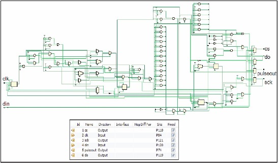
Figure 10. RTL Scheme of Combined Program for Pulse Generation, Over Current Protection and Setting Pulse Width from External Potentiometer
The drive pulse signal generated by FPGA board is shown in Figure 11 (a). The rise time and fall time of drive pulse are observed as less than 20 ns which are shown in Figure 11 (b) and Figure 11 (c) respectively. This drive signal has 3.3 V amplitude and 2.5 ms pulse width at 50 Hz frequency. The drive signal generated from FPGA board is given to signal translator unit and gate driver in pulsed output channel. The rise time and fall time of gate drive signal from gate driver are observed as < 500 ns, which are shown in Figure 12 (a) and Figure 12 (b) respectively. The amplitude of this gate drive signal is +15/-8 V. Twenty four numbers of 50 V, 80 A pulsed output channels of this pulsed power supply, whose drive pulses are generated by this FPGA based control and protection unit, are simultaneously tested on dummy resistive load. The waveforms showing output pulses of 4 numbers of 50 V, 80 A pulsed output channels on 1 ms, 10 μs and 100 ns time scales are given in Figure 13 (a), Figure 13 (b) and Figure 13 (c) respectively. From Figure 13 (c), it is clear that these output pulses are having a time delay of 60 ns among them which is negligible against their 2.5 ms pulse width and hence, these 4 output pulses are properly synchronized. However, this small time delay is caused by some minor dissimilarity among signal translator units, gate drivers and power path lengths of various pulsed output channels. The waveforms of one output pulse, its rise time and fall time are shown in Figure 14 (a), Figure 14 (b) and Figure 14 (c) respectively. The rise time and fall time of output pulse are observed as less than 20 μs. The inductances present in the power circuit of pulsed output channel play significant role in increasing the rise time and fall time of output pulse to 20 μs from 500 ns at output of gate driver. The voltage across MOSFET switch in pulsed output channel is shown in Figure 15 (a). The voltage overshoot across MOSFET switch during its turn OFF operation is observed as < 64 V, which is shown in Figure 15 (b). This voltage overshoot can be further reduced by increasing the value of snubber components but no efforts are made in this direction as it is well within acceptable limit. The voltage droop in the output pulse can be calculated as Δv = I x Δt/C. Here, C = 888 x 22000 μF = 19.536 F, Δt = 2.5 ms and I = 24 x 80 = 1920 A. So voltage droop is numerically calculated as, Δv = 245.7 mV. Figure 16 shows the waveform for voltage droop of 248 mV in output pulse which is less than 0.5% of 50 V. This droop is well within the acceptable limit of pulsed SSPA, which can be further minimized by increasing input capacitance value.
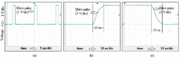
Figure 11. Drive Pulse Signal Generated by Spartan-6 FPGA Development Board (a) Output Pulse of 2.5 ms ON Time at 50 Hz, (b) Rise Time < 20 ns, (c) Fall Time < 20 ns
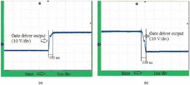
Figure 12. Gate Drive Pulse Signal Generated by Gate Driver (a) Rise Time < 500 ns, (b) Fall Time < 500 ns
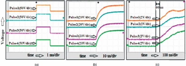
Figure 13. Synchronized Output Pulses of 4 numbers of 50 V, 80 A Pulsed Output Channels (a) 1 ms Time Scale, (b) 10 μs Time Scale (c) 100 ns Time Scale
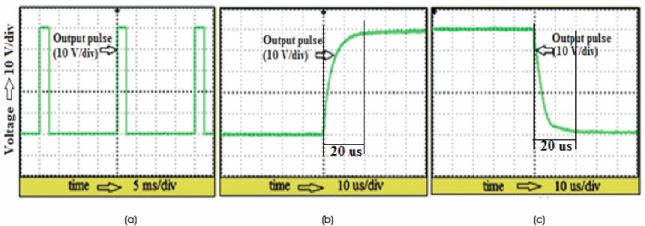
Figure 14. Output Pulse Waveform During Simultaneous Testing of 24 numbers of 50 V, 80 A Pulsed Output Channels (a) Output Pulse (2.5 ms ON Time @ 50 Hz), (b) Rise Time < 20 μs (c) Fall time < 20 μs
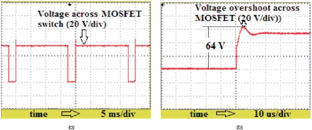
Figure 15. (a) Voltage Across MOSFET Switch in Pulsed Output Channels, Pulse ON Time 2.5 ms and OFF Time 17.5 ms (b) Voltage Overshoot Across MOSFET Switch During Turn OFF < 64 V
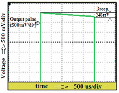
Figure 16. Voltage Droop in Output Pulse
An FPGA based control and protection unit employing Xilinx make XC6SLX9TQG144C FPGA has been developed to generate synchronized drive pulses for driving 24 numbers of 50 V, 80 A pulsed output channels of a multichannel pulsed power supply for biasing pulsed solid state RF amplifiers. This control and protection unit also protects pulsed output channels from over current condition. The rise time and fall time of drive pulses generated by this FPGA, which operates at 50 MHz clock frequency, are observed as less than 20 ns. This assists in reducing the rise and fall time of output pulses of all pulsed output channels. The wire lengths in the power paths of all pulsed output channels are kept same for reducing the jitter among output pulses. During testing of pulsed output channels on dummy load, the rise time and fall time of output pulses are observed as < 20 μs for pulse duration of 2.5 ms at 50 Hz repetition rate. The typical jitter among output pulses of different pulsed output channels is observed as 60 ns only. The voltage overshoot across MOSFET switch in pulsed output channel during its turn OFF operation is observed as < 64 V. Voltage droop in output pulse is observed as < 0.5% which is in close agreement with calculated value.