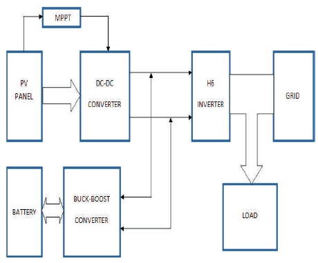
Figure 1. Block Diagram Representation of Proposed Topology
The photovoltaic technology is one of the base sources of distributed generations for future generation, but it lacks certainty in power production. Absence of transformer in DC/AC conversion will reduce the cost and volume of the PV inverter. The absence of transformer creates galvanic isolation problem that produces leakage currents between grid and PV panel. The grid connected PV inverters with bipolar SPWM is able to supply active and reactive power to grid. The bipolar SPWM has high switching losses and voltage stress across the filter inductor, which is double the supply voltage. The conventional unipolar SPWM mitigates voltage stress and switching losses, but it lacks reactive power capability. In this paper, a new topology is proposed to give solutions to the above mentioned problems associated with reliability, leakage currents, and reactive power capability in a single topology. A transformerless H6 inverter is used to reduce leakage currents. A modified unipolar SPWM technique is applied to H6 inverter to mitigate voltage stress and switching loss with reactive power capability. A battery storage system is also connected between PV panel and inverter to make PV system reliable at least in power supply.
Photovoltaic technology is one of the base sources of distributed generations for future generation, where the photovoltaic effect is totally dependent on atmospheric conditions. So, it lacks certainty in power production. Grid connected PV inverters with storage will give reliable power supply during night times and grid failures. There are different storage options like Compressed Air Energy Storage (CAES), batteries, Pumped Hydro Storage (PHS), super capacitors, etc. Both PHS and CAES methods are used for high power storage (in orders of Mega Watts) and requires distinctive geographic and geological necessities (Denholm & Kulcinski, 2004). So PV inverters with battery storage (Linden & Reddy, 2002) is the ideal choice for PV systems. There are different PV configurations for grid integration (Freddy & Rahim, 2016). They are mainly divided into two categories such as with transformer and without transformer. Transformerless configuration is highly efficient, less cost, and small in size compared with the high frequency and low frequency transformer inverter topologies. In transformerless topology, leakage current problem is the main drawback. The Common Mode Voltage (CMV) and galvanic connection are main sources for leakage currents. Galvanic connection between PV panel and grid creates path for leakage currents. Galvanic isolation means No direct path to current flow. So a bypass branch should be connected on input side or on output side of PV inverter to create galvanic isolation. PV panel structure has a conducting material. So between PV panel and earth, parasitic capacitance exists. This parasitic capacitance and filter inductor of the inverter creates a resonant circuit. The oscillating nature of CMV charges and discharges the parasitic capacitance in the resonant circuit that creates high leakage currents. So leakage currents will be eliminated if we maintain constant CMV and galvanic isolation. Generally, the grid connected inverters manufacture with unit power factor design. According to VDE-AR-N4105 (Demirok et al., 2011), the grid tied PV systems must have reactive power capability. Bipolar SPWM maintains constant CMV and also it is able to operate at any power factor, i.e. inverters with bipolar SPWM technique has capability of supplying both active and reactive power with less leakage currents. One setback of bipolar SPWM is that for each switching state changeover, the voltage across the inductor changes from +VDC to –VDC i.e. double the supply voltage that causes high voltage stress, ripple currents, and switching loss, consequently, size of filter inductor increases and efficiency of PV inverter reduces.
Cost and efficiency are the crucial points in the PV inverter’s manufacturing market. So, Unipolar SPWM is the solution, but conventional Unipolar SPWM lacks reactive power capability. There are various papers presented on unipolar SPWM with reactive capability in (Yang, Blaabjerg, & Wang, 2014; Wu, Kuo, Sun, & Hsieh, 2014; Chen, Gu, Zhang, & Lai, 2016; Islam, Afrin, & Mekhilef, 2016; Barater et al., 2016; Xiao, Xie, Chen, & Huang, 2011). In (Islam et al., 2016), high efficiency is achieved with SiC diodes and MOSFET switches. But this circuit has complexity in design. Intermittence in power generation, efficient inverter and reactive capability are problems that are discussed individually in some papers. but a combined solution has not been proposed. And in (Freddy, Lee, Moon, Lee, & Rahim, 2017), Reactive power capability concept is analyzed with H5 and HERIC inverters and a modified unipolar SPWM was proposed, which has a reactive power capability, but they modeled PV panel as DC source and failed to analyze the reactive power capability with practical PV panel modeling and MPPT tracking.
In this paper, a combined circuit topology which gives a solution to the above mentioned problems is proposed and a modified unipolar SPWM technique along with its reactive power capability is analyzed with practical PV modeling and MPPT tracking considerations. And this modified SPWM technique is applied to the H6 inverter, which has less leakage currents, which proves validation of the proposed SPWM technique for any unipolar SPWM grid-tied inverters. The complete block representation of the new photovoltaic topology proposed is shown in Figure 1. Battery storage system is connected between PV panel and inverter. The battery stores energy during abundant irradiation conditions. There is discharge during reduced irradiation conditions. A simple voltage regulator (P controller) is used to maintain the constant DC link voltage during battery discharging operation.
Figure 1. Block Diagram Representation of Proposed Topology
The knowledge of Common Mode Voltage behavior is essential for understanding the transformerless inverter topologies. The operation of H6 inverter is analyzed with conventional and modified unipolar modulation in terms of reactive power capability.
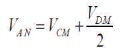
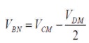
PV panel structure and earth creates parasitic capacitance. Due to galvanic connection and parasitic capacitance, leakage path exists. The leakage current path in transformerless inverters is shown in Figure 2(a). The voltage at point A with respect to neutral point and voltage at point B with respect to neutral point can be modeled as controlled voltage sources as shown in Figure 2(b). This parasitic capacitance and filter inductor of the inverter creates a resonant circuit which is shown in Figure 2(c). The Common Mode Voltage and differential mode voltages are defined as
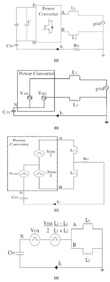
Figure 2. Common Mode Voltage Behavior
From equations (1) and (2),
The equivalent Common Mode Voltage is given by,
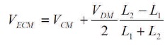
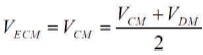
If we make L1 = L2, VDM effect will be eliminated. This is the reason for using two inductors in output side of the inverter.
From Figure 2(d) it is observed that CMV is like voltage applied to CPV and leakage current is the current flowing through CPV. So leakage current equation is approximately equal to current through the capacitor.
It is clearly observed that leakage current greatly depends on VCM. If the CMV is oscillating in nature, leakage currents will increase. And if we maintain constant CMV, leakage currents will be eliminated. But in unipolar SPWM during freewheeling period CMV is not constant. So by conclusion, leakage currents are not completely eliminated by galvanic isolation rather some other CMV clamping branch is needed to maintain constant CMV.
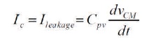
H6 topology is derived from H5 topology. An extra switch is connected between positive polarity of PV panel and B terminal of the inverter as shown in Figure 3(a). Generally, PV to grid connected systems operates under unity power conditions. The gate pulses for H6 inverter are shown in Figure 3(b). Vg is the grid voltage, Iref is grid current under unity p.f. Vgs1 to Vgs6 are the gate pulses to corresponding switches. Operation of H6 topology is divided into four modes.
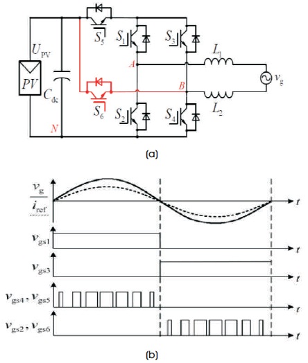
Figure 3. (a) H6 Inverter, (b) Conventional Gate Pulse Signals
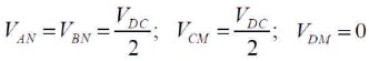
Mode-1: In Figure 4(a), During mode1 S1, S4, S5 switches are in ON state and switches S2, S6, and S3 are in OFF state. Inverter current direction is through S1, S5 and switch S4.
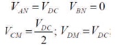
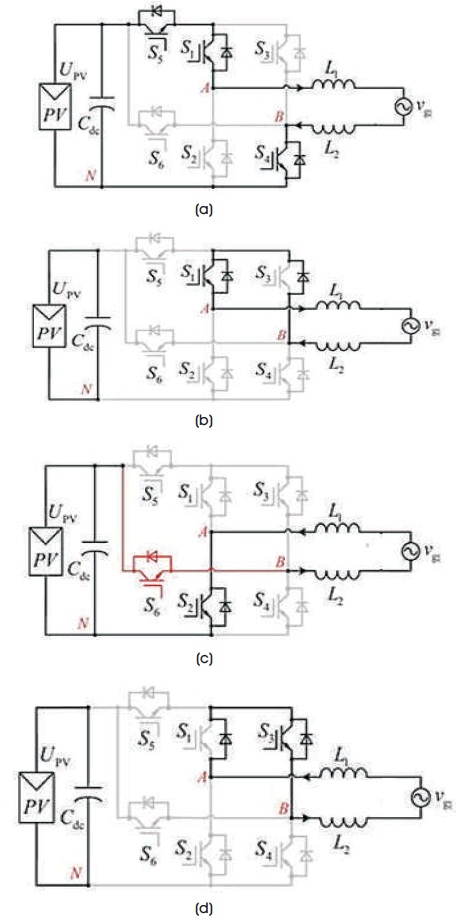
Figure 4. (a) Mode -1, (b) Mode - 2, (c) Mode -3, (d) Mode -4
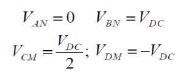
Mode-2: In mode-2 see in Figure 4(b), S1 is in ON state. Remaining switches are in OFF state. In freewheeling operation, inductor current freewheels through the anti-parallel diode of S3 and switch S1. VBN starts decreasing and VAN starts increasing, both settles at a voltage of VDC/2.
Mode-3: In mode-3 as shown in Figure 4(c), S2 and S6 are ON and other switches are in OFF state. Inverter current direction is in the opposite direction to the mode-1 current.
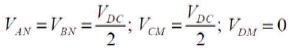
Mode-4: In mode-4, see in Figure 4(c), S3 is ON, remaining switches are in OFF state. The inductor current Freewheels through anti-parallel diode of S1 and switch S3. VBN starts decreasing and VAN starts increasing, both settle at a voltage of VDC/2.
It is observed that CMV is oscillating in mode-2 and mode- 4. So leakage current is more during freewheeling period compared with the conduction period (mode-1 and mode-3).
Unipolar modulation gives output voltages, such as +VDC, 0, -VDC and 0 V magnitudes consequently, which is why unipolar modulation is also called three level modulation. From the above 4 modes, we got +VDC, 0, in positive half DC cycle, -VDC, and 0 V in negative half cycles consequently. DC So, it can be concluded that the conventional unipolar PWM in Figure 3(a) works good for transformerless inverters under unity p.f.
In addition to the four modes, one extra mode exists under non-unity power factor condition. For example, under lagging p.f. condition, in reactive power region freewheeling path must be created to get zero voltage situations. During reactive power period in negative half cycle as shown in Figure 5(a), Ig is positive, Vg is negative. Inductor current has no path to freewheel so output voltage is only -VDC in the same way during reactive power period in positive half cycle as in Figure 5(b), i.e. Ig is negative and Vg is positive. Inductor current has no path to get 0 V state. So output voltage is only +VDC.
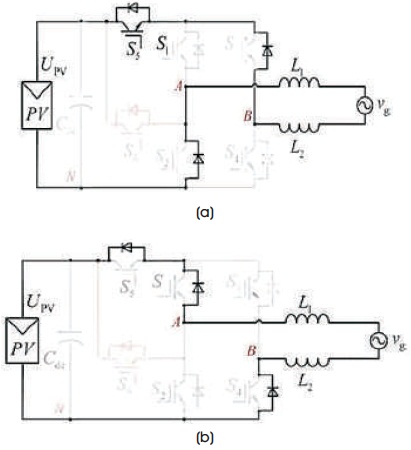
Figure 5. (a) Period-ii with Conventional PWM , (b) Period-iv with Conventional PWM
Hence the conventional SPWM in Figure 3(b) is not suitable for non-unity p.f. condition, i.e. conventional SPWM has no reactive power capability.
The proposed PWM pulses (Freddy et al., 2017) are shown Figure 6(a), where individual reference signals are needed to generate the proposed PWM. Sinusoidal signal is taken as VREF and triangular wave is taken as carrier signal.
During reactive power region in period-II, zero voltage state is achieved by commuting S3 complimentarily with switch S4 as shown Figure 6(c). Then a freewheeling path is created through S1 and anti-parallel diode of S3 switch. In period-IV, zero voltage state is achieved by commutating S1 complimentarily with switch S2 as shown Figure 6(d).
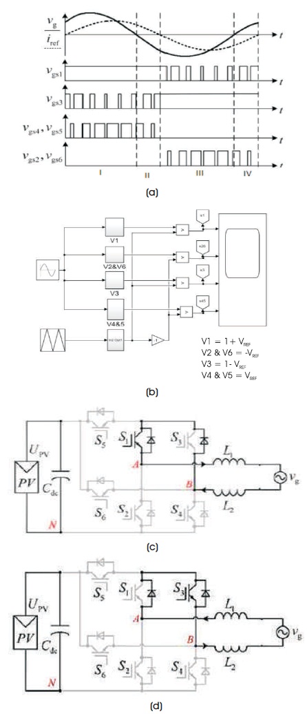
Figure 6. (a) Modified Gate Signals, (b) Gate Signals Generation Strategy, (c) Zero Voltage State during Period-ii, (d) Zero Voltage State during Period-iv
Then a freewheeling path is created through S3 and anti- parallel diode of S1 switch. By conclusion it is proved that modified unipolar SPWM technique has the capability of reactive power supply under non unity p.f.
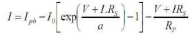
The electrical equivalent model of PV module is shown in Figure 7. It is the practical modeling with both series and parallel resistances Rs and Rp.
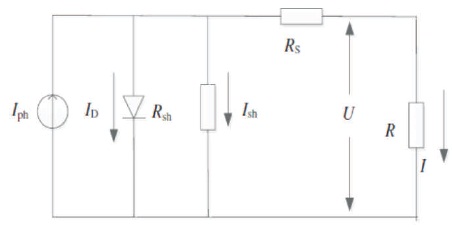
Figure 7. Equivalent Circuit of PV Module

where, Iph is the photovoltaic current, ID is current through diode, and Ip is leakage current through Rp .
Equation (9) gives the best results and almost equal to the practical values. In this paper, equation (9) is modeled with basic Matlab/Simulink blocks. I-V and P-V characteristics of PV model is shown in Figure 8. In the graph, MPP is the Maximum Power Point at which maximum power can be tracked. S simple Perturb and Observe algorithm is used to get maximum power. A DC to DC converter is used to implement the MPPT control.
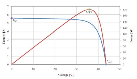
Figure 8. I-V and P-V Characteristics of PV Module
Among different storage methods for PV systems, battery storage is the ideal choice to use as a storage system. In this paper, Matlab/Simulink battery block is used. Battery is connected to PV panel with a buck-boost converter. Battery is charged during irradiance conditions (1000 W/m2) and discharged during low irradiation (0 W/m2) conditions. To implement the switching operation between charging and discharging modes, a simple logic switch is used from Matlab/Simulink library. The SOC of battery is taken as 50% and a simple Proportional (P) controller is used to maintain constant DC link voltage.
Simulation results are done in Matlab/Simulink software with parameters as mentioned in Table 1. BP MSX 120 Datasheet is used to implement the PV model. Single BP MSX 120 module gives 42.1 open circuit voltage. In this paper, 10 modules are connected in series and Inverter DC link voltage is maintained with 400 V. 1000 W/m2 and 0 W/m2 Irradiation conditions are given as input by using signal builder. Battery is charged during 1000 W/m2 condition and discharged during 0 W/m2 irradiance condition. 25 0C is taken as reference temperature. A simple P controller is used to maintain 400 V DC link voltage during battery discharge.
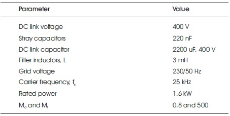
Table 1. Parameters of Inverter
Figure 9. (a) Conventional PWM Results, (b) Proposed PWM Results
Figure 10 shows battery state of charge characteristics. Up to 0.2 s, 1000 W/m2 is given as input to PV panel. So, the battery is charged for 0.2 s and discharged after 0.2 s. Figures 11 to 13 show the grid current and grid voltage under unity p.f, 0.8 lagging p.f and 0.8 leading p.f respectively with conventional and proposed SPWM. In addition to the reactive power capability, transient state is also examined. Figure 14 gives transient state from 0.8 lagging to 0.8 leading p.f. Figure 15 shows the leakage currents under transient condition.
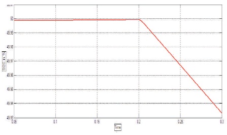
Figure 10. Battery State of Charge (SOC)

Figure 11. (a) Conventional Results under Unity p.f, (b) Proposed Results under Unity p.f
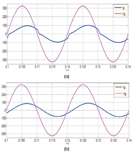
Figure 12. (a) Conventional Results under Lagging, (b) Proposed Results under Lagging p.f
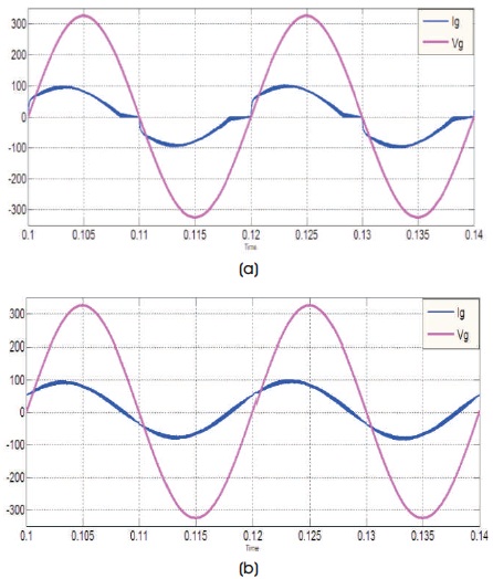
Figure 13. (a) Conventional Results under Leading p.f, (b) Proposed Results under Leading p.f
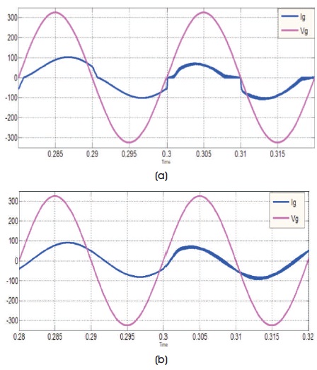
Figure 14. (a) Conventional Transient Results in Vg and Ig from Lagging to Leading p.f, (b) Proposed Transients Results in Vg and Ig from Lagging to Leading p.f.

Figure 15. (a) Conventional Transient Results for Leakage Currents from Lagging to Leading p.f., (b) Proposed Transient Results for Leakage Currents from Lagging to Leading p.f.
Any PWM computability can be checked out by observing the inverter output voltage before filters. Unipolar SPWM has to produce +VDC and 0 voltage states consequently for positive AC voltage and also –VDC and 0 voltage states consequently for negative AC voltage. Figures 9(a) and (b) show the inverter output before filter with conventional and proposed SPWM techniques, respectively. On careful observation, during reactive power region, there is no 0 voltage state in Figure 9(a), whereas Figure 9(b) has 0 voltage states in all regions.
Hence, it is proved that the proposed unipolar SPWM technique has reactive power capability.
In this paper, reliability, reactive power capability, and efficient PV inverter configuration are combined into a single circuit topology. Battery is used to mitigate uncertainty in power supply. Modified unipolar SPWM and its reactive power capability is analyzed with transformerless H6 inverter which has less leakage currents.
PV panel is modeled with equation (9), which gives more practical performance than the DC voltage source as PV model. From the simulation results it is proved that the modified unipolar SPWM has better results for reactive power and it can be applied to any transformerless inverters, which are using conventional unipolar SPWM technique, without any changes in the inverter circuit design. Hence the proposed PV topology would give satisfactory performance.