Figure 1. Circuit Diagram of SEPIC Converter
This paper presents different topologies applied to the Single ended primary inductor converter (SEPIC) to obtain high static gain, and an overview of different types of converters. Nowadays, there is requirement of high efficiency in DC-DC converters for better performance of appliances. Hence, so many techniques are developed in order to increase the static gain of DC-DC converters for high efficiency and also high power solutions. New alternatives in SEPIC converter have been proposed for high and very high step-up ratio applications, which are based on new topologies known as modified SEPIC converters. These modifications give high static gain in comparison with the existing SEPIC converter and other classical converters.
The power converters are used for the conversion, control and conditioning of electric power, in which the power varies up to megawatts as in electric power transmission system. These are power electronics circuits, in which the electronic devices and control circuits must be highly robust to achieve a long useful life and the total efficiency of the power electronic circuits must be as high as possible. The most common classification of power converters is as follows:
AC to DC converters are also known as rectifiers. It converts alternating current (AC) signal to direct current (DC) signal and the process of converting AC signal to DC signal is called rectification.
DC to AC converter are also known as inverters. It converts the Direct Current signal into Alternating Current signal. Thus the inverter performs the opposite function of rectifier and can obtain a certain amplitude and frequency of the AC voltage or current.
AC to AC converters are also known as AC Voltage Controllers and Cyclo-Converter. These are employed to transform an AC input signal to an AC output signal with variable amplitude. Depending on the converter complexity, the frequency can be changed using Cyclo- Converter.
DC-DC converters are also known as Choppers. It converts fixed DC input into a variable DC output. DC-DC converters are the basic converters in switch mode power supplies.
DC-DC converters are classified as follows:
Buck Converters are also known as Step-Down Converters. The average output voltage is less than the input voltage in Buck converter. It is made up of a voltage source, a switch, a diode, an inductor, a capacitor and a resistive load.
The Boost Converters are also known as step-up Converters. The average output voltage is greater than the input voltage in Boost Converter. It has similar structure as the Buck converter, the only the difference is that, it has components arranged in a different manner to obtain the output voltage greater than input voltage.
Buck-Boost converters are the combination of Buck and Boost converter. It provides output voltage less than or greater than the input voltage. The components of Buck- Boost converter are similar, but arranged in a different way to provide step up and step down voltage.
Cuk converters are also the combination of Buck and Boost converter. The output of the Cuk converter is inverted, as it transfers the energy through the capacitor, whereas the Buck, Boost and Buck-boost converters transfer the energy through the inductor.
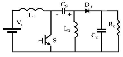
Single ended primary inductor converters allows the electrical potential i.e. voltage at its output to be greater or less than its input. The output of this converter is controlled by the duty cycle of the switch. The SEPIC converter exchanges energy between the capacitors and inductors, in order to convert one voltage to another. The amount of energy exchanged is controlled by switch S. The energy to increase the current IL1 comes from the input source. The power circuit of the SEPIC converter is presented in Figure1.
Figure 1. Circuit Diagram of SEPIC Converter
When the switch is ON it acts like a short circuit, and the instantaneous voltage VCS is approximately Vi. The voltage VL2 is approximately –Vi . Therefore, the capacitor CS supplies the energy to increase the magnitude of the current to IL2 which increases the energy stored in L2 .
When switch S is turned OFF, the current ICS becomes same as the current IL1 , since inductors not allow instantaneous changes in current. The power is delivered to the load from both L2 and L1 . CS , however, is being charged by L1 during this OFF cycle, and will in turn recharge L2 during the ON cycle.
There are so many techniques, which are developed in order to increase the static gain of the DC-DC converters for high efficiency and high power solutions. New alternatives for high and very high step-up ratio applications are proposed. The different topologies obtaining high static gain and high efficiency in SEPIC converter are as follows:
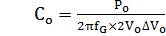
The modified SEPIC converter is accomplished by including the diode DM and the capacitor CM in basic SEPIC converter as presented in Figure 2.
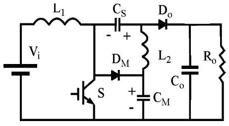
Figure 2. Circuit Diagram of Modified SEPIC Converter
The first stage of operation varies from time t0 to t1 . At the instant t0 , the switch S is turned-off, and the energy stored in the input inductor L1 is transferred to the output through the capacitor CS and output diode DO, and also to the capacitor CM through the diode DM. Therefore, the switch voltage is equal to the capacitor CM voltage. The energy stored in the inductor L2 is transferred to the output through diode D0 .
The second stage of operation varies from time t1 to t2 . At the instant t1 , the switch S is turned-on and the diodes DM and DO are blocked, and the inductors L1 and L2 store the energy. The input voltage is applied to the input inductor and the voltage VCS −VCM is applied to the inductor L2. The voltage VCM is higher than the voltage VCS . [1-2]
The operating waveform of modified SEPIC converter is presented in Figure 3.
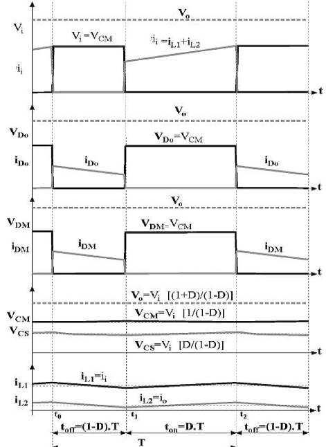
Figure 3. Operating Waveforms of Modified SEPIC Converter
The voltage in all diodes and the power switch is equal to the capacitor CM voltage. The output voltage is equal to the sum of CS and CM capacitors' voltages. The average L1 inductor current is equal to the input current and the average L2 inductor current is equal to the output current.
The static gain of the modified converter can be obtained by considering the average inductor voltage as zero at the steady state. Therefore, the relation presented in (1) must occur at the steady state for the inductor L1 .


Therefore, CM capacitor voltage is defined by (3), which is M the same equation of the classical boost static gain given by,

During the period, where the power switch is turned (toff ), the diodes DM and D0 are in conduction state, and the following relation can be defined :

The L2 average voltage is zero at the steady state, and the following relations can be considered:


From the equations (3), (5) and (6), the static gain of the proposed converter is obtained and presented in (8)

From the above equation, we get the duty ratio which is given by:

The voltage of the series capacitor (VCS ) is defined by substituting (3) and (8) in (7), resulting the following equation:

For a classical SEPIC converter, the static gain is given as follows, which is the same as the equation (10), because the output voltage is equal to the capacitor CS voltage. Thus the static gain of the classical SEPIC converter is given by:

From above equation, we get the duty ratio for classical SEPIC converter, which is given by:

The switch voltage for the classical SEPIC converter is equal to the sum of the input and output voltages. Therefore, the operation voltage is very high, mainly in maximum input voltage condition. The switch voltage of the modified SEPIC converter is equal to the voltage of capacitor CM. This voltage is determined by (3) as follows:

The input inductance value is defined as a function of the maximum input current ripple. As the classical SEPIC, boost, and the modified SEPIC converters present the same input stage, the equation for the determination of input current ripple is the same for all converters. The input current ripple (ΔiL1 ), during the conduction of the power switch is defined by the following equation:

where, f is the switching frequency.
The input current ripple (ΔiL1 ) is defined from (14) and presented in (15). Replacing in (14) the input current ripple is obtained as.

The input inductance can be defined by (16) obtained from (15). The input inductance is calculated for the power converter, operating at the peak of the lowest input voltage. The input inductance calculated is equal to,

The CS series capacitor and the CM multiplier capacitor cannot be as large as the output filter capacitor CO. However, these present a high-frequency voltage ripple due to the circulating current and the capacitor charge variation ΔQ. As the circulating current in both capacitances are equal, the high frequency voltage ripple is the same. During the power switch turn-on period, the current in CS and CM capacitances is equal to the L2 inductor current. The capacitor charge variation ΔQ is calculated as,

The high-frequency capacitor voltage ripple ΔVC can be defined as a function of the capacitor charge variation.

Therefore, CS and CM capacitances can be defined as

where, f is the switching frequency and C=CS =CM
The output capacitance is calculated as given below:
The magnetic coupling allows increase of the static gain with a reduced switch voltage as presented in Figure 4 which shows low switch voltage and high efficiency for low input voltage and high output voltage applications.
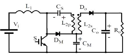
Figure 4. Modified SEPIC Converter with Magnetic Coupling
The modified SEPIC converter without magnetic coupling can operate with double the static gain of the classical Boost converter for a high duty-cycle. However, a very high static gain is necessary in some applications. A practical limitation for the modified SEPIC converter is overvoltage at the output diode DO , due to the existence o of transformer L2 leakage inductance.
This overvoltage is controlled with the inclusion of a voltage multiplier at the secondary side as shown in Figure 5. This voltage multiplier increases the converter static gain, the voltage across the output diode is reduced to a value lower than the output voltage and the energy stored in the leakage inductance is transferred to the output. Therefore the secondary voltage multiplier is composed of diode DM2 and capacitor CS2 which is also a non- dissipative clamping circuit for the output diode.
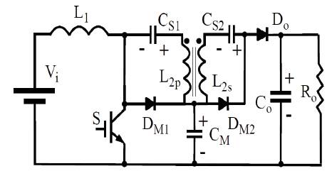
Figure 5. Modified SEPIC Converter with Magnetic Coupling and Output Diode Voltage Clamping.
These topologies can operate with high static gain and reduced switch voltage. The commutation losses of the proposed converter with magnetic coupling are reduced, due to the presence of the transformer leakage inductance and the secondary voltage multiplier that operates as a non dissipative clamping circuit to the output diode voltage. [3]
The key components in power conversion are the magnetic devices, which are used in the two forms of 1) transformers and 2) coupled inductors. These two devices have distinct functions: transformers realize the instantaneous transfer of energy from one port to other and coupled inductors store energy incoming from the ports during a time interval and deliver it out through the same ports during a different time interval.
The modified SEPIC converter with coupled inductors is shown in Figure 6. The operation of this converter consists of charging the inductors Li and Lo during the first part of the switching period, taking the energy respectively from the input and from the Coupling capacitor Cc and discharging them simultaneously into the load through the rectifier, during the second part of the switching period. If too small, the Coupling capacitor Cc can be responsible for a voltage imbalance between the two inductors, which makes the design of switching regulators based on SEPIC topology not trivial, mainly because of the instability issues in current controlled applications with input voltage spanning a wide range.
Figure 6. Modified SEPIC Converter with Coupled Inductors
The output depends on the coupling factor of coupled inductors, the capacitance of the coupling capacitor, and the conversion ratio in SEPIC topology. Using the coupled inductors, an appropriate coupling capacitor is required to prevent big input and output ripple currents. This modified topology provides higher static gain than the ordinary SEPIC converter and also predicts the ripple and the appropriate size of the coupling capacitor. [4- 7]
The other topology is the combination of SEPIC converter and high gain multilevel Boost converter as shown in Figure 7. In this topology, only one input source and switch are required to obtain two output voltages at the same time. One output voltage is obtained through high gain multilevel Boost converter and other output voltage is obtained through SEPIC converter. SEPIC converter operates in two modes, step-up or step-down depending on the duty cycle.
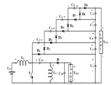
Figure 7. SEPIC Converter with Multilevel Boost Converter
The operation of SEPIC based dual output DC-DC converter can be divided into two modes, when switch S is turned ON and another when switch S is turned OFF. In mode 1, switch S is turned ON, the inductors L1 and L2 are charged from the input source and capacitor Cs1 respectively. Capacitor C1 clamps the voltage across capacitor C2 through D2 and switch S, when D2 is forward biased. In mode 2, switch S is turned OFF, the inductors L1 and L2 discharge through D and D1. The inductor current and input voltage charges the capacitor CSO. The output voltage levels of high gain multilevel boost converter can be increased by adding diodes and capacitors without disturbing the main circuit. Dual Converters are useful, when dual output voltage levels are required from single input supply voltage. One input source and switch is required to obtain two output voltages at the same time. One output voltage is obtained through 5-level multilevel boost converter and the other output voltage is obtained through the SEPIC converter. [8-11]
A new topology for highly efficient step-up and step-down converter in continuous conduction mode with the inclusion of an auxiliary diode and switch, form a new direct power delivery path between input and output. By shortening the time period for the original SEPIC operation and increasing the time period for the direct power link operation, this converter can reduce the ripple currents and switching voltages of switches, diodes, and inductors.
This topology is shown in Figure 8. In this topology, there are two parts, the first part is the original SEPIC consisting of inductors L1 and L2 , capacitors Cin , Cout , and CS , a switch SW1, and a diode D1 . The second part is an additional circuit consisting of a diode D2 and a switch SW2 . The additional circuit provides a new power delivery path between input and output. D2 prevents reverse current from the output and SW2 controls the current flow of the modified SEPIC with Sw1.
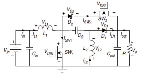
Figure 8. SEPIC Converter with Auxiliary Diode and Switch
With this new moification, much of the input power is directly delivered to the output with little losses. Ripple currents and switching voltages on circuit components are highly reduced. [12]
The new circuit of the coupled-inductor SEPIC converter is proposed by an addition of the secondary output inductor and a diode in a basic SEPIC converter, so that a new converter with a large conversion ratio is obtained as shown in Figure 9. The splitting of this secondary inductor into two windings, reduces the voltage stresses on the main switch and diodes. The output secondary winding is split into two windings, and a diode D3 and a capacitor C2 are added. Lm denotes the magnetizing inductance and Lk ,the leakage .
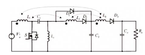
Figure 9. SEPIC converter with inductor and diode
The additional diode helps to circulate the leakage inductance energy to the load in a non oscillatory manner. The transistor turns on/off with soft switching. The voltage stress on both the transistor and diodes is less than the output voltage. [13-18]
A general boost converter is not suitable for high step-up applications and therefore has limited voltage step-up ratio. The solution is obtained by combining a boost converter with SEPIC converter. This new integrated boost- SEPIC (IBS) converter is shown in Figure10. It provides an additional step-up ratio, with the help of an isolated SEPIC converter. Since the boost converter and the SEPIC converter share a boost inductor and a switch, its structure is simple. Also the proposed IBS converter needs no current snubber for the diodes, since the transformer leakage inductor alleviates the reverse recovery.
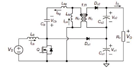
Figure 10. Integrated Boost-SEPIC Converter
The IBS converter is a combined operation of a boost converter and a SEPIC converter with a common boost inductor and a switch. Each converter is operated with its original function and an additional effect of the transformer leakage inductance Llkg . During the switch OFF state, Llkg forces commutation of the diode current lkg between two converters, slowly from the lower diode Do1 to the upper diode Do2 . The lower diode current can be decreased to zero or not depending on the turns ratio n, though both the inductor current ILb and ILm are continuous. [19-24]
This new topology of SEPIC converter is used in power factor correction circuits. The conventional SEPIC converter was primarily designed to provide a nonpulsating input current, operating with both inductors in continuous current mode and only the DC-DC conversion was considered. The modified SEPIC converter can be viewed as a cascade of a modified boost converter and a buck-boost converter. The switches are turned ON and OFF synchronously. The modified boost converter operates in discontinuous current mode, while the Buckboost converter operates in continuous current mode. Since a high power factor is naturally achieved in this way, a simple feedback scheme suffices to regulate the output as shown in Figure 11.
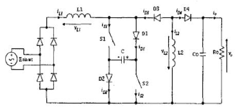
Figure 11. Modified SEPIC Converter as a Combination of Modified Boost and Buck-boost Converter
When the switches are ON (mode 1), both inductance currents flow through the switches and discharge the capacitor C. At the same time, the output capacitor Co is discharging on the load resistor. When the switches are OFF (mode 2), the current of Ll inductor flows through diodes Dl and DZ, and charges up the capacitor C, while the current of L2 inductors is forced into the free- wheeling diode D4 . When the value of L1 current becomes zero, the charging of the capacitor stops. The current of L2 keeps free-wheeling through D4 diode.
The cycle ends at the instant when the switches are turned ON again. The proposed converter can be a useful circuit for power factor correction, using a modified SEPIC converter, which can naturally achiev a high power factor and a simple circuit for the output regulation. [25]
A continuous conduction mode SEPIC converter with low reverse-recovery loss is proposed for power factor correction. The proposed SEPIC converter is shown in Figure 12, which can reduce the reverse recovery loss of diodes and improve the power efficiency. By utilizing a coupled inductor and an additional diode, zero-current turn-OFF of the output diode is achieved. The reverserecovery current of the additional diode is reduced by leakage inductance of the coupled inductor. The proposed SEPIC converter provides high power efficiency and high power factor compared to the conventional power factor correction circuits employing the SEPIC converter.
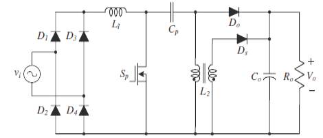
Figure 12. Modified SEPIC Converter by Utilizing a Coupled Inductor and an Additional Diode
The proposed converter can be divided into two parts. The first part is the continuous conduction mode SEPIC converter, composed of L1, L2, Cp, Co, Do, D1 –D4 , and Sp . The second part is an additional branch consisting of a diode Ds and the secondary windings of a coupled inductor L2 . The second part provides zero-current turn-OFF of the output diode Do. [26-30]
A single switch two diodes wide conversion ratio step down/up converter is presented in this proposed converter, which is derived from the conventional Single Ended Primary Inductor Converter (SEPIC) topology and it can operate into a capacitor-diode voltage multiplier, which offers simple structure, reduced electromagnetic interference (EMI), and reduced semiconductors voltage stress. This proposed converter is shown in Figure 13. It provides continuous output current, higher voltage conversion ratio, and near zero input/output current ripples compared with the conventional SEPIC converter. The proposed SEPIC converter with continuous output current and voltage-doubler characteristics is shown in Figure 13, which resembles the conventional SEPIC converter, except that its output port has been modified to include two identical capacitors C connected through two diodes followed by L3 Co filter.
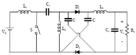
Figure 13. Modified SEPIC Converter with Continuous Output Current and Voltage-doubler Characteristics
The two capacitors C appear in a parallel configuration, during the switch OFF time. Hence, they are charged equally by the energy stored in the filter inductors L1 , L2 , and L3. During the switch ON time, the two capacitors C are discharged in series through the load and the filter inductor L2 . Thus, for the same duty-cycle, the proposed converter is capable of supplying an output voltage level twice as much as the conventional SEPIC converter. [31]
There is a requirement of large conversion rate in converters for many industrial applications. The requirements also includes good efficiency, little electromagnetic interference noise, operation at high switching frequency, and a small amount of elements. Also, switch mode power supplies are used widely in consumer electronic appliances. They are designed with intent to pass the electromagnetic compatibility certification test, which is mandatory and vital for some applications like telecommunication, automotive, and medical equipments. Designing high performance power converter with low cost, small size, and high efficiency makes the electromagnetic interference design a more challenging task. The designing task becomes even more difficult for applications that demand wide range of voltage gain with reduced input and output current ripple. For these applications, there are so many types of DC-DC converters and SEPIC converter is a type of these converters, but an ordinary SEPIC converter is not suitable for high step-up applications. Hence, so many topologies are discussed with an inclusion of different elements like as inductor, diode, transformer, switch etc. in ordinary SEPIC converter to obtain high step-up voltage i.e. high static gain.