Figure 1. High Efficiency MOSFET inverter with H6 type configuration.
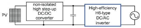
A novel, high-efficiency inverter using MOSFETs for all active switches is presented for photovoltaic, nonisolated, ac module applications. The proposed H6-type configuration features high efficiency over a wide load range, low ground leakage current, no need for split capacitors, and low-output ac-current distortion. A two stages ac module combining non isolated high step up converter and high efficiency inverter with H6 type configuration is used to solve the aforementioned issues. The two stages configuration can significantly reduce the power decoupling capacitance by locating the capacitor in dc link. Detailed power stages operating principle, PWM scheme and novel bootstrap power supply for proposed inverter are described when the unipolar PWM scheme in used a transformer less PV system.
Photo Voltaic (PV) ac modules may become a trend for future PV systems because of their greater flexibility in distributed system expansion, easier installation due to their “plug and play” nature, and higher system-level energy harnessing capabilities under shaded or PV manufacturing mismatch conditions as compared to the single or multi string inverters. A number of inverter topologies for PV ac-module applications have been reported so far with respect to the number of power stages, location of power-decoupling capacitors, use of transformers, and types of grid interface [3]. Unfortunately, these solutions suffer from one or more of the following major drawbacks: the limited-lifetime issue of electrolytic capacitors for power decoupling, limited input voltage range for the available panels in the market, high ground leakage current.
When the unipolar Pulse Width Modulation (PWM) scheme is used in a transformer, less PV system and low-system efficiency if an additional high-frequency bidirectional converter is employed and increased cost and complexity of the circuit if energy in the transformer leakage inductance is recycled by either an active snubber (or) soft switching circuit.
The detailed power stage operating principles, Pulse Width Modulation scheme, associated multilevel bootstrap power supply, and integrated gate drivers for the proposed inverter are described. 50% reduction of the output inductance as compared to that of the common full-bridge inverter with bipolar PWM switching, low output ac current distortion because the PWM dead time for the Proposed circuit is eliminated; and the simple bootstrap power supply and the integrated gate drivers for the presented inverter. Experimental results of a 300W hardware prototype show that not only are MOSFET (Metal Oxide Semiconductor Field Effect Transistor) body diode reverse-recovery and ground leakage current issues alleviated in the proposed inverter, but also that 98.3% maximum efficiency and 98.1% European Union efficiency of the dc–ac power train and the associated driver circuits are achieved .
Figure 1. High Efficiency MOSFET inverter with H6 type configuration.
This paper, however, will concentrate on the second power stage—the inverter circuit is to obtain high efficiency of the MOSFET DC-AC circuit and to avoid the high Ground leakage of the current issue [7]. The simplest inverter using hybrid MOSFETs and Insulated Gate Bipolar Transistors (IGBTs) with unipolar PWM to achieve high efficiency is shown in Figure 1. The high-side IGBTs serve as line frequency polarity selection switches and low-side MOSFETs operate in high frequency Sinusoidal PWM (SPWM) to control the output voltage or current. The high efficiency of the hybrid four-switch inverter can be achieved over the wide load range because the MOSFETs can avoid the fixed voltage-drop losses and significantly reduce the turn-OFF losses without tail current as compared to the case with IGBTs.
However, the hybrid four-switch inverter with unipolar PWM is not suitable for nonisolated ac-module application, because the high ground leakage current is generated through the parasitic capacitance of the PV panel due to the high-frequency voltage which is swing at the PV terminals. The severe ground leakage current results in problems, which include lower efficiency, output current distortion, ElectroMagnetic Interference (EMI) and safety issue [2]. The proposed inverter with H6-type configuration, which is composed of six power MOSFETs (S1–S6), two freewheeling diodes (D1 and D2), and two split inductors (L1 and L2) act as a low-pass filter.
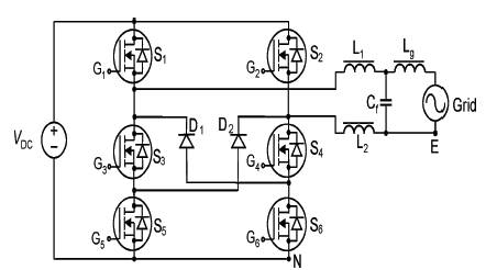
Figure 2. Circuit diagram
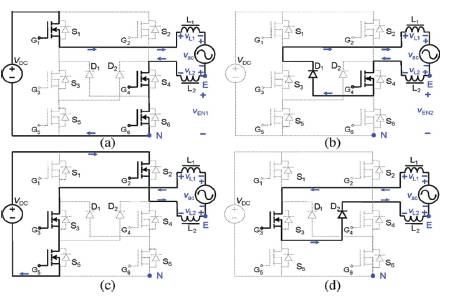
Figure 3. Circuit diagram of the proposed inverter
Figure 2. illustrates the PWM scheme for the proposed inverter. The top device is in one leg and the bottom device in the other leg is switched simultaneously in the PWM Cycle and the middle device operates as a polarity selection switch in the grid cycle, which is shown in Figure 2. If the sinusoidal control voltage control, which is synchronized with the output voltage, is higher than the triangular carrier voltage v carrier, then the gating voltage G1 and G6 are active; otherwise G1 and G6 are inactive. If the control is higher than zero, the gating voltage G4 is active; otherwise, G4 is inactive.
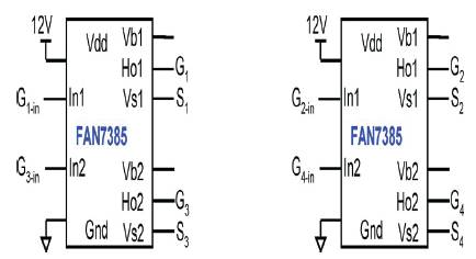
Figure 4. Gate driver
Similarly, the comparison of the carrier or zero results in the logical signals to control G2 , G5 , and G3 , respectively. The four topological stages in one grid cycle for the proposed inverter is mentioned in the paper. Note that the point N is the dc-link negative terminal, and the point E is the grid negative terminal. The four operating modes are briefly described as follows. During the grid is positive half cycle, switch S4 remains ON, whereas S1 , S6 , and D1 commutate at the PWM switching frequency. When S1 , S6 , and S4 are ON and the other switches and diodes are OFF, the inductor current is charging, as shown in Figure 3.
Although the proposed inverter has distinctive advantages over the conventional full-bridge inverter, there are also some shortcomings associated with this method: two more active switches and their gate drivers and the individual power supplies. Multilevel bootstrap technology has been presented in the multilevel inverter. The major technology issue of this kind of bootstrap circuit is, its dependence on the power train topology and the corresponding PWM scheme. In this paper, the authors apply the technique to the proposed power circuit using the cross-leg connection for charging path.
The high-side and middle-side MOSFETs in the same phase leg can be driven by one of the FAN7385 integrated circuits, as shown in Figure 4. The high-side and middle-side MOSFETs in the same phase leg can be driven by one of the FAN7385 integrated circuits.
Such a cost-effective solution to power the high-side and mid-side Gate drives for the proposed inverter using the bootstrap power supply technique is shown in Figure 4. Four small capacitors Ca1 –Ca4 and diodes Da1 –Da4 are employed to transfer the energy to the high-side and midside switches from an auxiliary voltage source Ea . Note that the energy of Ca1 cannot be transferred from Ca3 , which is in the same phase leg because the middle device S3 and its body diodes are never turned on. S1 operates at high frequency, such that the cross-leg connections of the bootstrap circuit for the proposed inverters are necessary. As shown in Figure 4 when the inverter output voltage is positive, the capacitor Ca4 is charging through Da4 at every PWM cycle since the low- side switch S6 in the same leg is turned on at high frequency. With the cross-leg connection, Da3 can be turned on before D1 is ON at every PWM cycle, while S4 remains ON like what the high-side drive in the normal buck converter does, as shown in Figure 4. Thus, energy of Ca4 can transfer to Ca1 through Da3 to turn ON the high-side switch S1 . The proposed cross-leg bootstrap power supply is preferred to the use of isolated auxiliary supply for each gate drive because of its compact size and compatibility with integrated chips. It makes the proposed inverter more appealing for PV ac-module applications.
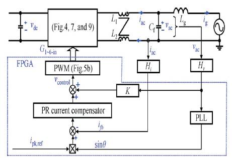
Figure 5. Output filter
The first consideration is the type of the output filter. The proposed design is to adopt two split inductors at the inverter output to allow the equal voltage swing over the two inductors so that the high-frequency voltage swing between the PV negative terminal and the grid ground can be reduced significantly if the inductance values are identical. The physical structure shown in Figure 5 can minimize the difference of inductance because, Figure 5 it is Symmetric inverter-side inductors:
The symmetrical windings of the split inductors share the same Core to avoid the effect of the magnetic variation. In order to attenuate more switching ripple for the gridside current, additional capacitor Cf and inductor Lg can be added to form a second-order filter, as shown in Figure5. The second design consideration is the current control strategy effect on the output filter design. The design needs to consider the position of feedback signals and the current loop compensation. As shown in Figure, by selecting the voltage at the filter capacitor Vac and the current of the inverter-side inductor Iac as the feedback signals with admittance feed forward compensation, the entire 2 LCL current control plants can be simplified as a first-order system under the condition that the capacitor Cf is small enough to be negligible. Figure 5 shows the block diagram of the complete inverter. More detailed analysis about the controller design can be referred in the third design consideration which is filter-parameters calculation, which can be determined by setting criteria on ripple current and filtering criteria .The inverter-side inductance can be calculated based on the design criterion that the maximum magnitude of the peak-topeak current ripple is less than10%–20% of the rated output current I rated in the whole grid cycle. The peak-topeak inductor current ripple can be derived as

Where,
Vdc-direct voltage.
Vac-alternating voltage[6].
D- Duty cycle.
Ts- PWM switching period.
L1& L2-indutance.
Δipk-The peak-to-peak inductor current ripple.
A 300W hardware prototype has been designed, fabricated and tested to verify the validity of the proposed inverter which is targeted at PV nonisolated ac-module application. The main devices S1 -S6 are 250 V, 42.5 mΩ MOSFETs (FDB2710), the freewheeling diodes D1 and D2 are ultra fast diodes CMR5U-04 (400 V/5 A), the auxiliary diodes Da1 - Da4 are ultra fast diodes MURA160 (600 V/1 A), and the bootstrap capacitors Ca1 ∼ Ca4 are 1 μF, 25 V X7R. A 2 LCL filter is shown in (L1 + L2 = 1.6mH, Cf = 0.68 μF, and Lg = 0.5mH) which is used as the output filter. The three pieces of dual-channel high-side gate driver integrated chips FAN7385 with the proposed bootstrap power supply are designed to produce the matched gating signals for the six power MOSFETs. Specifications of the inverter are as follows: battery bank voltage Vdc = 180–200 V; output power Po = 300 W; grid voltage Vg, rms = 120 V; switching frequency Fsw = 30 kHz. A digital control board with Spartan-3E FPGA is used as the sinusoidal output current controller (Figure 7). The experimental gating signals in the grid cycle and in PWM cycle are shown in Figures 4,5 respectively. It can be seen that the experimental gating signals vG1, vG6, and vG4 agree with the analysis results of the PWM scheme and the proposed bootstrap circuit works well by observing that the gate drive voltage level of the middle and top switches are kept constant during the grid cycle. Moreover, the gate drive signal vG1 of the top switch in one leg and the vG6 of the bottom switch in the other leg are matched with each other. The experimental switches voltage waveforms under 200V dc-link conditions are shown in Figure 7. The voltage stress of the top switch S1 and the middle switch S4 is 200 V, which is the same as the dc-link voltage[1]. The voltage stress of the bottom switch S6 is about half of the dc-link voltage, as shown in Figure 7. The switches S1 and S6 almost evenly share the dc-link voltage when they switch OFF simultaneously. The experimental waveforms of the ground potential is under full-load conditions. The testing results of the ground potential agree with the (6). The high ground leakage current is avoided by observing that the high-frequency voltage of the ground potential is less than 10 Vrms under full load conditions. The experimental waveforms of the grid current under the 200 Vrms grid voltage and full-load conditions are described in Figure 7. This figure shows that the proposed inverter presents the high power factor and low harmonic distortion. This paper illustrates the experimental results for efficiency under different dc- the link voltages and output loads with 30-kHz switching frequency and 120 Vrms ac voltage condition.
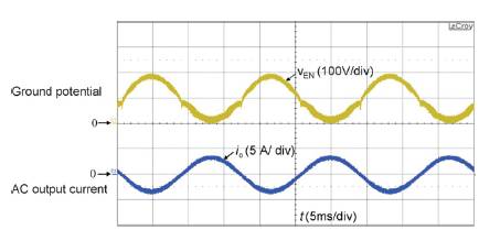
Figure 6. Experimental waveforms of the ground potential and ac output current under full load condition.
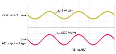
Figure 7. Experimental waveforms of the grid current under the grid Voltage and full-load conditions.
This paper proposes a novel single-phase inverter [8] with H6-type configuration as a part of a wide input range, high efficiency, and long life time PV nonisolated 300Wac module. Key features of the proposed circuit are as follows [4] [5] [9-11]