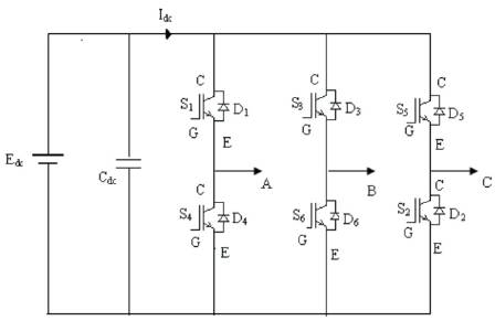
Figure 1. Three phase voltage source inverter
The usage of non-linear loads like variable speed drives, SMPS, UPS, etc., connected to power systems cause the harmonic currents which make sinusoidal currents/voltages to non-sinusoidal currents/voltages. Harmonic voltage results from the harmonic currents interacting with the impedance of the power systems, which results in the power quality problem. In this research paper, the harmonic levels of a sinusoidal pulse width modulated two level three-phase inverter are compared with the sinusoidal pulse width modulated three level inverter. The three-phase three level diode clamp inverter is designed and simulated using PSpice and the DSP based hardware model is developed using IGBT as the power devices. The hardware model is tested for resistive load, which results are obtained with the help of Fluke 434 power quality analyzer. In this multilevel inverter the magnitude of the fundamental component is increased and the total harmonic distortion decreased by 50% for both practical and simulated cases, when compared to the threephase two level conventional PWM inverter.
An inverter is commonly used in variable speed AC motor drives to produce a variable three-phase AC output voltage from a constant DC voltage source, which has two voltage level (+VDC , -VDC ). The output waveform of inverters should be sinusoidal for efficient operation. But the output of conventional two level PWM inverters would be a square wave (or) quasi square wave. The square wave is rich in harmonic content. To minimize the output voltage distortion with improved fundamental voltage, the multilevel inverter concept has been implemented. The concept of utilizing multiple small voltage levels (multilevel) to perform power conversion was patented by an MIT researcher over twenty years ago. The first topology introduced was the series H-bridge design by Baker [1]. This was followed by the diode clamped converter which utilized a bank of series capacitors. These designs can create higher power quality for a given number of semiconductor devices than the fundamental topologies alone due to a multiplying effect of the number of levels.
These multilevel inverters are suitable for high voltage and high power application due to their ability to synthesize waveforms with better harmonic spectrum. Numerous topologies have been introduced and widely studied for utility and drive applications. Multilevel pulse width modulated (PWM) inverters are gaining importance due to the fact that the lower order harmonics in the output waveform can be eliminated without any increase in the higher order harmonics, unlike the regular two level PWM inverters. Multilevel inverters provide more than two voltage levels. As the number of levels reaches infinity, the output Total Harmonic Distortion (THD) approaches to zero. This inverter generates almost sinusoidal staircase voltage with only one time switching per line cycle. In this chapter the comparative performance of the three level, three phase diode clamped inverter with the conventional two level, three phase voltage source inverter was carried out for both the simulated and hardware models.
Nabae et al and Bhagwat and Stefanovic presented the general idea behind the multilevel converter technology is to create a sinusoidal output voltage from several small voltage steps [2] [3]. There are several advantages to this approach when compared with traditional two-level converters. Traditional 2-level high-frequency pulse width modulation (PWM) inverters for motor drives have several problems associated with high frequency switching, which produce common-mode voltages and high voltage change rates to the motor windings. The smaller voltage steps lead to the production of higher quality waveforms (therefore a multilevel converter distinguishes itself by being the converter with the lowest demands on the input filters) and also reduce the stresses; the seriestype connection of the semiconductors allows operation at higher voltages. Brumsickle et al stated that the switching frequency of the multilevel converter could be reduced to 25% of the switching frequency of a two level converter[4]. These converters recently have found many applications in the medium and high power applications. Large electric drives will require advanced power electronics inverters to meet the high power demands required of them. Advantages of this multilevel approach include good power quality, good electromagnetic compatibility (EMC), low switching losses, and high voltage capability. One clear disadvantage of multilevel power conversion is stated by Stemmler et al, and Kawabatta is the larger number of semiconductor switches required, however lower voltage rated switches can be used and the active semiconductor cost is not significantly increased when compared with the two level case[5] [6]. The most commonly reported disadvantage of the multilevel converters is that, a larger number of switching semiconductors are required for lower-voltage systems and the small voltage steps must be supplied on the DC side either by a capacitor bank or isolated voltage topologies. When isolated voltage sources are not available, series capacitors require voltage balance. According to Strzelecki et al [7], for three level converters this problem is not very serious because the voltage balancing can be overcome by using redundant switching states, which exist due to the high number of semiconductor devices.
Diode-clamped multilevel inverters are very similar to the conventional back-to-back voltage source inverters. Even though having a larger number of switches it should be pointed out that in a three level converter the voltage rating of the transistors is half that of the transistors in a two level converter. Furthermore, the switching losses, which are reduced by the lower transistor blocking voltage and increased by the higher number of transistors, for this converter will be lower than that of a two level converter. Additionally, it should be noted that each transistor switches only during a portion of the network period, which again reduces the switching losses. Grzegorz Benysek [8] stated that for three level converters maintaining voltage balance on the capacitors can be accomplished through selection of the redundant switching states which lead to the same output voltages, but yield different capacitor currents. In this thesis a three level, three phase diode clamped converter has been developed and its performance is compared with the performance of the two level, three phase voltage source inverter for both simulation and hardware.
The standard three-phase voltage source inverter is shown in Figure1 and the eight valid switch states are given in Table 1. As in single-phase VSIs, the switches of any leg of the inverter (S1 and S4, S3 and S6, or S5 and S2) cannot be switched on simultaneously because this would result in a short circuit across the DC link voltage supply. Similarly in order to avoid undefined states in the VSI, and thus undefined AC output line voltages, the switches of any leg of the inverter cannot be switched off simultaneously as this will result in voltages that will depend upon the respective line current polarity. Of the eight valid states, two of them (7 and 8 in Table 1) produce zero AC line voltages. In this case, the AC line currents freewheel through either the upper or lower components. The remaining states (l to 6 in Table 1) produce non-zero AC output voltages. In order to generate a given voltage waveform, the inverter moves from one state to another. Thus the resulting AC output line voltages consist of discrete values of voltages that are, 0, and. The selection of the states in order to generate the given waveform is done by the modulating technique that should ensure the use of only the valid states [9].
Figure 1. Three phase voltage source inverter

Table 1. Valid switching states for three-phase VSI
The IGBT based three-phase two level inverter is simulated using PSpice with sinusoidal modulation and it is shown in Figure 2. The inverter circuit has the following specifications: Input voltage =230V DC, Output voltage = 230V, 50Hz, three phase AC and load resistance = 360Ω per phase and its output line voltage waveform is shown in Figure 3. It may not be possible to reduce the overall voltage distortion due to harmonics but by proper switching control the magnitudes of lower order harmonic voltages can be reduced, often at the cost of increasing the magnitudes of higher order harmonic voltages. Such a situation is acceptable in most cases as the harmonic voltages of higher frequencies can be satisfactorily filtered using lower sizes of filter chokes and capacitors. Many of the loads, like motor loads have an inherent quality to suppress high frequency harmonic currents and hence an external filter may not be necessary. Unlike in square wave inverters the switches of PWM inverters are turned on and off at significantly higher frequencies than the fundamental frequency of the output voltage waveform. Figure 4 shows the harmonic spectrum for simulation of three-phase two level inverter.
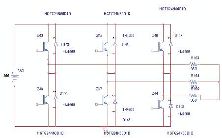
Figure 2. PSpice model of three-phase two level inverter
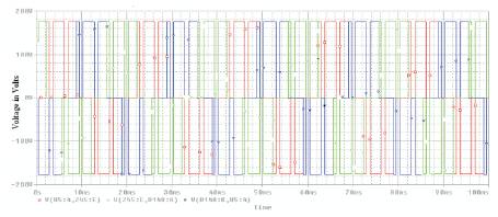
Figure 3. Output line voltage waveforms for threephase two level inverter
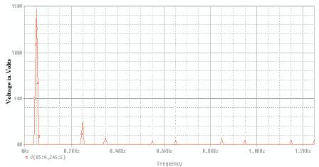
Figure 4. Harmonic spectrum for three-phase two level inverter
The hardware model is implemented for the three-phase two level inverter using TMS 320LF2407 DSP processor for the same specifications mentioned in the previous section. The DSP processor is used to generate the gating signals. The hardware model is tested for a three-phase resistive load (360 ohms in each phase) and the test setup is shown in Figure 5. The results are recorded by using a fluke 434-power quality analyzer. The output line line voltage waveform is shown in Figure 6. The harmonic spectrum of the output lineline voltage and individual harmonic distortion levels are shown in Figures 7 and 8 respectively. The comparison between the simulation results and hardware results are shown in Table 2.
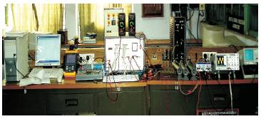
Figure 5. Hardware test setup of two level inverter
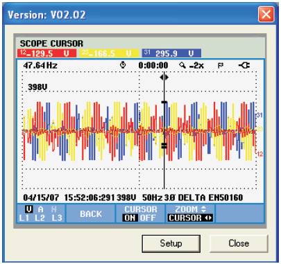
Figure 6. Output line-line voltage waveforms
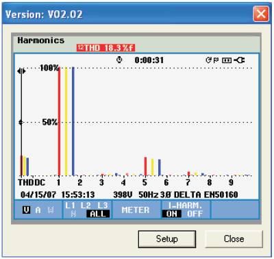
Figure 7. Harmonic spectrum of the line line voltage waveforms
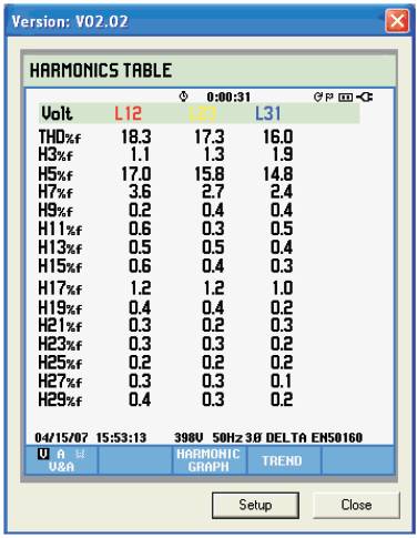
Figure 8. Percentage harmonic distortion of individual harmonic levels
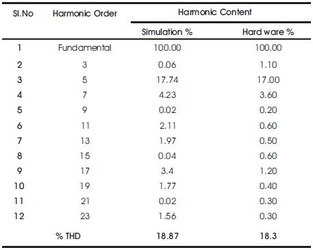
Table 2. Comparative analysis of % harmonic distortion of output voltage waveform in both simulated and hardware results
Recently the “multilevel inverter” has drawn tremendous interest in the power industry[10]. The general structure of the multilevel inverter is to synthesize a sinusoidal voltage from several levels of DC voltage sources, typically obtained from DC-bus capacitor/voltage sources. A three-level inverter, also known as a neutral-clamped inverter, which consists of two capacitor voltages in series and uses the center tap as the neutral. Each phase leg of the three-level converter has two pairs of switching devices in series. The center of each device pair is clamped to the neutral through clamping diodes. The waveform obtained from a three-level inverter is a quasisquare wave output.
The diode clamp method can be applied to higher-level inverters. As the number of levels increases, the synthesized output waveform adds more steps, producing a staircase wave which approaches the sinusoidal wave with minimum harmonic distortion. Ultimately, a zero harmonic distortion of the output wave can be obtained by an infinite number of levels [11].
In three level inverters, the switching of the upper and lower devices in a half-bridge inverter generates Va0 wave with positive and negative levels (+0.5Vd and -0.5Vd ), respectively. If the fundamental output voltage and corresponding power level of the PWM inverter are to be increased to a high value, the DC link voltage Vd must be increased and the devices must be connected in series. By using matched devices in series, static voltage sharing may be somewhat easy, but dynamic voltage sharing during switching is always difficult. The problem may be solved by using a multilevel, Neutral clamped inverter [12].
The diode-clamped inverter provides multiple voltage levels through connection of the phases to a series bank of capacitors. According to the original invention, the concept can be extended to any number of levels by increasing the number of capacitors. Early descriptions of this topology were limited to three-levels [13], where two capacitors are connected across the DC bus resulting in one additional level. The additional level was the neutral point of the dc bus, so the terminology neutral point clamped (NPC) inverter was introduced. However, with an even number of voltage levels, the neutral point is not accessible, and the term multiple point clamped (MPC) is sometimes applied [13]. Due to capacitor voltage balancing issues, the diode-clamped inverter implementation has been mostly limited to the threelevel. Because of industrial developments over the past several years, the three-level inverter is now used extensively in industry applications [14]. Although most applications are medium-voltage, a three-level inverter for 480V is on the market.
The basic configuration of a three-level three-phase diode clamped inverter is shown in Figure 9. In this configuration the DC link capacitor C has been split to create the neutral point 0. Since the operation of all the phase groups is essentially identical, consider only the operation of the half-bridge for phase a. A pair of devices with bypass diodes is connected in series with an additional diode connected between the neutral point and the center of the pair as shown in Figure 9. The devices Q1 and Q4 function as main devices (like a twolevel inverter), and Q2 and Q3 function as auxiliary devices which help to clamp the output potential to the neutral point with the help of clamping diodes D1 and D2 [15].
The phase voltage Va0 waveform with three angles and the corresponding gate voltage switching waves as shown in Figure 10. The main devices (Q1 and Q4) generate the Va0 wave, whereas the auxiliary devices (Q3 and Q2) are driven complementary to the respective main devices, with such control, each output potential is clamped to the neutral potential in the off periods of the PWM control, as indicated in the Figure 10. Evidently, positive phase current +ia will be carried by devices Q1 and Q2 when Va0 is positive, by devices D3 and D4 when Va0 is negative, and by devices D1 and Q2 at the neutral clamping condition. On the other hand, negative phase current- ia will be carried by D1 and D2 when Va0 is positive, by Q3 and Q4, when Va0 is negative, and by Q3 and D2 at the neutral clamping condition. This operation mode gives three voltage levels (+ 0.5Vd , 0, - 0.5Vd ) at the Va0 wave, compared to two levels (+0.5Vd and -0.5Vd ) in a conventional two level inverter. The levels of line voltage wave Vab are +Vd , - Vd , +0.5Vd , - 0.5Vd and 0 compared to levels +Vd , -Vd and 0 in a two-level inverter. Therefore, the three-phase inverter has 33 = 27 switching states but there are only eight states are available for a two level inverter. The Line- Line voltage waveform is shown in Figure 11 [12].
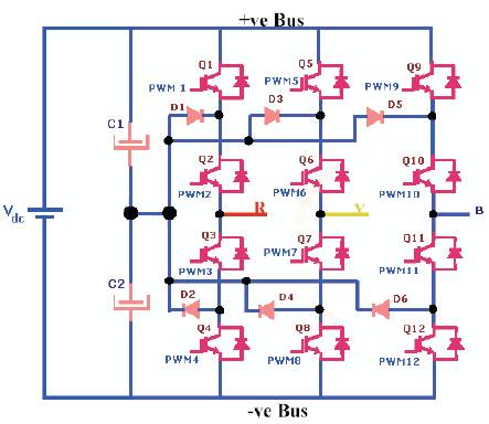
Figure 9. Power circuit of three phase three-level diode clamped inverter
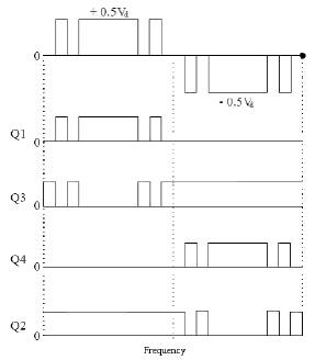
Figure 10. PWM signals for switching devices of R phase
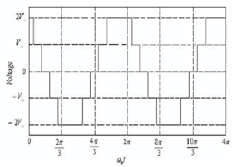
Figure 11. Line-line voltage waveform
Three-Phase Three Level Diode clamp inverter has been simulated using PSpice and their results are verified with the developed hardware model. Figure 12 shows the simulated power circuit model for three-phase three level diode clamped multilevel inverter. The phase voltage and the line to line voltage of the simulated model are shown in Figures 13,14 respectively. The harmonic spectrum of the output line-line voltage is shown in Figure 15.
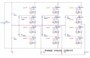
Figure 12. PSpice simulation of three-phase three level diode clamped inverter
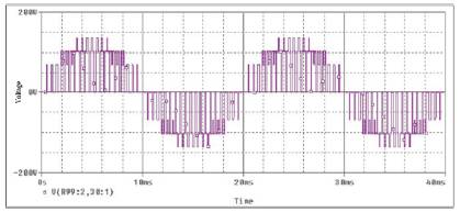
Figure 13. Output phase-neutral voltage of three level diode clamped inverter
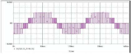
Figure 14. Output line-line voltage of three level diode clamped inverter
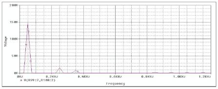
Figure 15. Harmonic spectrum for output voltage of three level diode clamped inverter
The hardware model of the three-phase three-level diode clamped multilevel inverter is implemented by using TMS320LF2407 DSP Processor. The hardware description of the system is shown in Figure 16. The hardware model contains a diode bridge rectifier, power circuit, optocoupler, gate drive circuitry, current sensor and signal conditioner. The input of diode bridge rectifier is 230V, 50Hz AC supply. KBPC 3510 device is used as diode bridge rectifier. An isolation transformer is a transformer, often with symmetrical windings, which is used to decouple two circuits. An isolation transformer allows an AC signal or power to be taken from one device and fed into another without electrically connecting the two circuits. Isolation transformers block transmission of DC signals from one circuit to the other, but allow AC signals to pass. They also block interference caused by ground loops. Isolation transformers are commonly designed with careful attention to capacitive coupling between the two windings. This is necessar y because excessive capacitance could also couple AC current from the primary to the secondary. A grounded shield is commonly interposed between the primary and the secondary. Any remaining capacitive coupling between the secondary and ground simply causes the secondary to become balanced about the ground potential.
To obtain the output voltages in three steps per leg are 0 Vdc /2, and Vdc. Thus for a three-phase inverter there are 27 states in total. Table 3 gives overall switching states of the inverter. In this structure (M-1)X2X3 switching devices,(M- 1)X(M-2) X3 clamping diodes and capacitors are used. (S1, S4), (S4,S8) and (S9,S12) are the main switches, they are switched directly by control pulses. (S2,S3), (S6,S7) and are the auxiliary switches and allow connection of the output of each phase to neutral point. The circuit is designed for the output voltage of three-phase, 230V, 50Hz. The IGBT1 MBH15D is used as power switching device.
The developed hardware model of three-phase threelevel diode clamped inverter with DSP processor is shown in Figure 17. The hardware model is tested for a threephase resistive load (360 ohms in each phase) and the test setup is shown in Figure 18. The gating pulses are generated using TMS 320LF2407 DSP processor and all R, Y and B phase PWM signals are observed as shown in Figures 19, 20 and 21 respectively. The output lineline voltage waveform is shown in Figure 22. The harmonic spectrum of the output lineline voltage and its harmonic level table for different odd harmonic orders are shown in Figures 23 and 24 respectively. The comparison between the simulation results and hardware results are shown in Table 4.
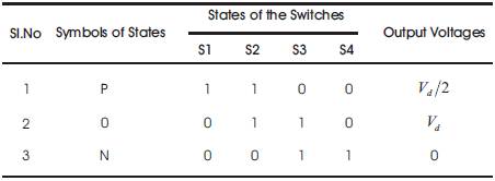
Table 3. States of the switches for one leg of inverter
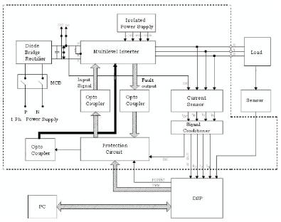
Figure 16.Hardware description of three level diode clamped inverter
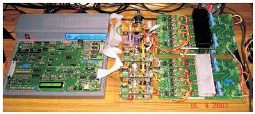
Figure 17. Hardware model for three-phase three level diode clamped inverter
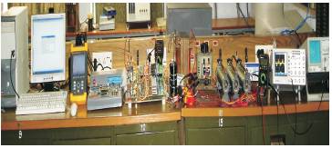
Figure 18. Test setup for hardware model of three level diode clamped inverter
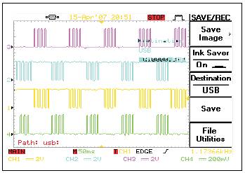
Figure 19. Hardware PWM pulse R-phase
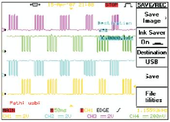
Figure 20. Hardware PWM pulse Y-phase
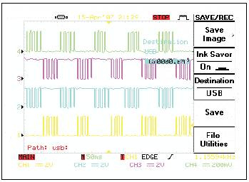
Figure 21. Hardware PWM pulse B-phase
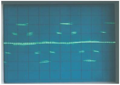
Figure 22. Output line-line voltage of three level diode clamped inverter
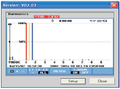
Figure 23. Harmonic spectrum of line-line voltage
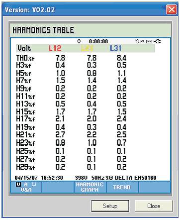
Figure 24. Percentage harmonic distortion of individual harmonic levels
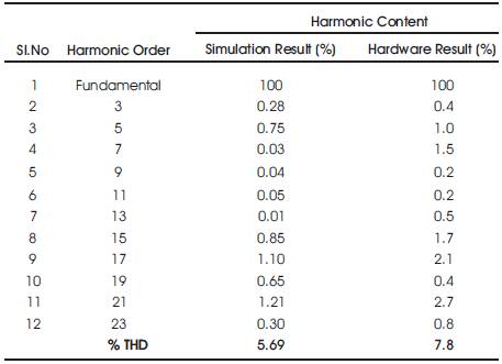
Table 4. Comparative analysis of % harmonic distortion of output voltage waveform for both simulated and hardware results
In multilevel inverters the power switches of lower voltage can be used to obtain desired voltages. These are faster and smaller than the power switches of high voltage, which is used in two level inverters. Multilevel inverters offer better sinusoidal voltage waveform than two voltage levels. This causes the Total Harmonic Distortion (THD) to be lower. Switching losses are reduced because switching frequency can be lower than that of two level inverter and also the switching speed is faster. Conduction losses are also lower because of low forward-voltage drop. When several voltage levels are used, the dv/dt of the output voltage is smaller thus the stress in cables and motors is smaller. The energy per cycle is more in the three level inverter when compared to two level inverter.
In the determination of inverter configuration, usually the cost comparison of different configuration has to be executed. The cost of the inverter is affected mainly by the DC-link capacitor, IGBT and the filtering components, while rests of the electronic component have quite insignificant affects. The good estimation of inverter costs can be done by comparing the cost of IGBT and Capacitor. In general, the two-level configuration is 30% cheaper than the three-level configuration. The difference is mostly due to the cost of clamping diodes, which are not needed in two-level configuration. The cost comparison is not taking account the effect of the volume to the unit prices. The effect of volume will decrease the unit price, which can affect to the relation between total costs.
The hardware and Pspice model of three-phase two-level sine PWM inverter is compared with hardware and PSpice based model of three-phase three-level diode clamped inverter. The harmonic levels of the different odd harmonic for both hardware model of conventional two level PWM inverter and three-phase three level diode clamped inverter as shown in Table 5.
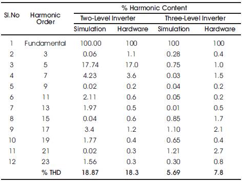
Table 5. Comparative analysis of % harmonic distortion in two level and three level inverter
The multilevel inverter topology can overcome some of the limitations of the standard two-level inverter. Output voltage and power increase with number of levels. Harmonics decrease as the number of levels increase. In addition, increasing output voltage does not require an increase in voltage rating of individual force commutated devices. The three level diode clamp inverter is discussed in detail with experimental results to verify the simulated results. The performance of the proposed three level diode clamp inverter is compared with the conventional two level inverter for both experimental and simulated results. The three level inverter, total harmonic distortion reduced by 57.38% as compared with two level inverter. Three level inverter can work at a very low switching frequency, which gives the possibility to work with low speed semiconductors, and to generate low switching frequency losses.