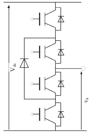
Figure 1. Different three-level inverter topologies, a. neutral point clamped, b. flying capacitor, c. h-bridge.
The paper presents a modular multi-cell three-level five-phase voltage source inverter. The topology is an extension of a single-phase H-bridge inverter. Positive and negative voltage levels are obtained by operating two switches at one time while zero voltage level is obtained by shorting the load side. The source side shorting is avoided in order to protect the source. The major advantage is multi-level output without capacitor voltage or neutral voltage balancing in contrast to the more commonly used neutral point clamped type and flying capacitor type. The major disadvantage from the industrial application point of view is the requirement of five isolated dc sources. Mathematical model is derived and presented. Modulation is obtained using simple phase disposition and level shifted sinusoidal carrier based scheme. A five-phase induction machine is considered as load and excitation and loading transient is presented. The simulation model considered the effect of dead-band in the switching signals. Further the effect of change in DC link voltages of different cells are also investigated and reported. The simulation and experimental results are shown.
Recently, multilevel converters have attracted attention in medium voltage and high power applications due to reduced voltage stress on power semiconductor switches, reduced voltage harmonics and electro magnetic interferences [1-4]. For higher voltage and high power applications, the switching frequency and device ratings are limited. Currently, multilevel converters are commercialized in standard and customized products that power a wide range of applications, such as compressors, extruders, pumps, fans, grinding mills, rolling mills, conveyors, crushers, blast furnace blowers, gas turbine starters, mixers, mine hoists, reactive power compensation, marine propulsion, High-Voltage Direct- Current (HVDC) transmission, hydro-pumped storage, wind energy conversion, and railway traction, to name a few [5-8]. Although it is an enabling and already proven technology, multilevel converters present a great deal of challenges, and even more importantly, they offer such a wide range of possibilities that their research and development is still growing in depth and width. Application of multilevel converter fed multiphase machines are still under development stage and it is the focus of the present day research [9-16]. Researchers all over the world are contributing to further improve energy efficiency, reliability, power density, simplicity, and cost of multilevel converters, and broaden their application field as they become more attractive and competitive than classic topologies.
During the last decade, multiphase machines have experienced growing interest due to several attractive advantages such as high reliability, fault tolerance, improved torque performance, and higher power density, which makes them especially suitable for marine/naval propulsion systems [9-10]. Hence, the combination of multiphase and multilevel technologies adds up a series of advantages that are useful for high power drives application. However, reliability is also a key ingredient in the future development of multilevel converters for multiphase machines. Some multilevel converter topologies have sufficient degrees of freedom to operate under the internal fault condition, with few added hardware. Nonetheless, the possibility to actually use this strength relies on the ability (accuracy and speed) to detect and diagnose a fault, so the fault-tolerant reconfiguration of the converter can be performed before damage generated by the fault takes place. Since capacitor faults and semiconductor short- or open-circuit faults occur so fast and due to the amount of power involved in these applications, it is still not practically feasible with the present state of technology to have a completely functional fault detection–diagnosis– operation system that is fully reliable [17-18].
Figure 1. Different three-level inverter topologies, a. neutral point clamped, b. flying capacitor, c. h-bridge.
The popular multi-level inverter topologies are Neutral Point Clamped (NPC), Flying Capacitor (FLC) type and cascaded Hbridge inverter Figure 1. Among the three topologies, the first two are employed for drives applications while the third is used in renewable energy system such as for interfacing solar PV to the grid. The major problems with NPC and FLC are the neutral point voltage fluctuation. The proposed topology is based on modular structure called Multi-Cell Topology. Each cell offer three-level single-phase output voltage waveforms. The major advantages are the modularity of the structure and no neutral point voltage fluctuation problem.
The topology presented in this paper consists of five identical cells. Each cell consist of four controlled power semiconductor switches with anti-parallel diodes. Each cell is supplied by a controlled or uncontrolled AC/DC converter. The AC/DC converter of each cell must be isolated from one another. The requirement of isolated DC supply system is one of the major drawback of the proposed topology. The proposed topology is modular and flexible, by adding a cell, the number of phases can be increased. The cells can be connected in series/cascade to enhance the number of levels as well. The proposed topology finds its applications in renewable energy interface in addition to motor drive system. The proposed topology for a five-phase motor drive application is shown in Figure 2.
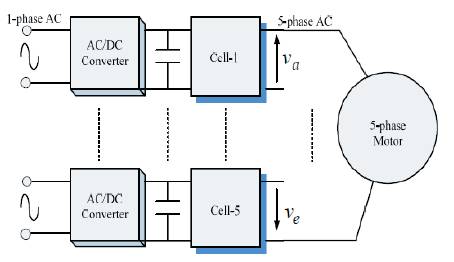
Figure 2. Five-cell based five-phase motor drive system
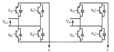
Figure 3. Five-cells of a five-phase 3-level inverter
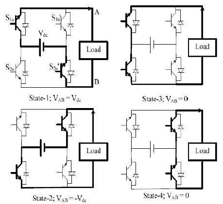
Figure 4. Switching states of one phase of a 3-level, PUC inverter.
The five cell structure is shown in Figure 3. The complimentary switches are shown by prime sign and the suffix relate to the switch number and output phase such as S1a and S1a’ belong to phase ‘a’. The switching operation of one cell is presented in Figure 4.
The output of the inverter is given as;
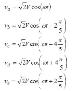
The working of a single-phase 3-level inverter can be described with the help of the following switching diagram shown in Figure 4. The switching states are shown in Table 1. From Table 1 it is seen that there are two switching states that are redundant. Four switching combination is possible with output voltage level as ±Vdc and 0. The shorting of dc source is avoided and hence the switches a dead band is provided between the switching on and off of the complimentary switches.
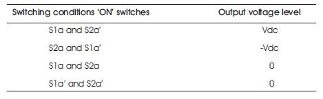
Table 1. Switching state of Cell-1
The presented topology generate 3-level output voltage wave form from a power electronic converter with very simple structure. The proposed topology do not need any extra clamping diodes or capacitors to generate 3-levels. In contrast, the existing topologies need diodes and/or capacitors to generate additional voltage level. The control structure is also very simple and can be easily implemented in low cost microcontrollers, embedded controllers, Digital Signal Processors (DSP) and Field Programmable Gate Arrays (FPGAs).
The proposed topology can be used as single-phase or multi-phase (more than 1 phase). The structure is modular and just by adding individual cells, the number of phases can be increased. Hence in this way, one can generate 3- phase or 5- phase, 6-phase etc. The control code is to be changed accordingly.
In order to obtain variable voltage and variable frequency output from the inverter, appropriate PWM scheme is needed. The most popular are sinusoidal carrier-based and space vector PWM. This paper present simple sinusoidal carrierbased PWM scheme. In multi-level inverter two types of sinusoidal carrier-based schemed are generally employed namely; level shifted and phase shifted PWM [1]. In case of level shifted PWM, for three-level output two high frequency triangular carrier signals are needed with level shift (carrier-1 varies from 0 to 1, while carrier-2 varies from -1 to 0). In phase shifted carrier based PWM scheme, two high frequency triangular carriers are generated with a phase shift of 180.The PWM signal generation block schematic is presented in Figure 5, here only level shifted carrier signal is shown. Space vector PWM can also be implemented and that will be reported separately.
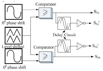
Figure 5. PWM signal generator with level shifted carrier signals
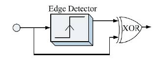
Figure 6. Dead band generator
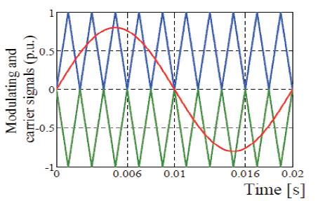
Figure 7. Level shifted Carrier-based PWM
A dead band is provided between the turning on and turning off of the complimentary switches as shown in Figure 6. The delay circuit provide dead band and the dead time is controlled from the edge detector by varying the sample time. In the results presented in this paper, dead band of 20 μs.74002134.
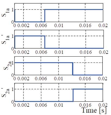
Figure 8. Switching signals or date signal for one cell
The PWM signal generation using level shifted carrier and sinusoidal modulating signal for a modulation index of 0.8 is shown in Figure 7. Carrier signal frequency is kept 10 times that of the modulating signals to generate this figure. The switching signals for the four switches are presented in Figure 8, considering switching at fundamental frequency i.e. at 50 Hz. The switching signals shown in Figure 8 verifies the operation of the cell as presented in Table 1.
The operation of a five-phase induction motor drive fed by five-cells voltage source inverter is validated by using Matlab/Simulink simulation. The simulation parameters are shown in Table 2.
Table 2. Simulation parameters
Equal DC link voltage is assumed for each cell equal to 300 V. Full rated voltage is thus applied to the motor terminals and is allowed to accelerate freely. A step load torque of 8.33 Nm is applied at t = 0.8 sec to investigate the load rejection behavior of five-phase drive system. The resulting simulation waveforms are presented in Figure 9.
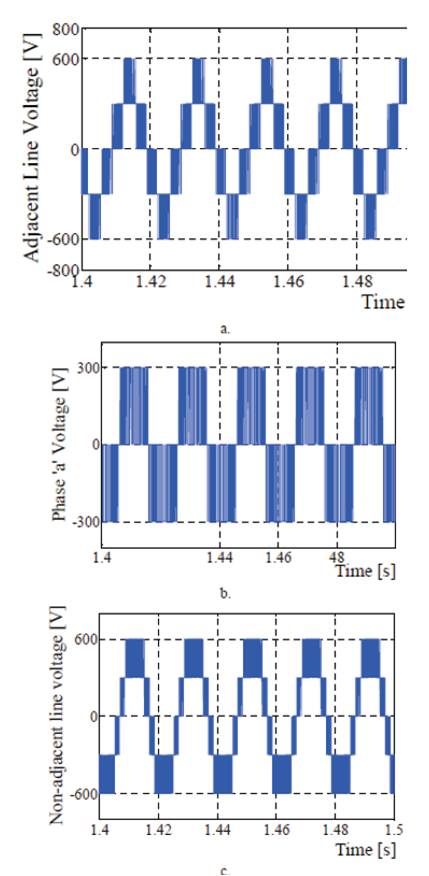
Figure 9. Output five-phase voltages of multi-cell inverter; a. adjacent line voltage, Vab, b. phase voltage ‘a’, c. non-adjacent line voltage, Vac
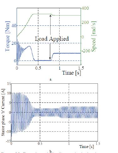
Figure 10. Five-phase induction motor behavior, a. Electromagnetic torque and speed, b. stator phase ‘a’ current
The torque and speed response of the five-phase induction motor supplied by five-cell inverter is presented in Figure 10a. A typical behavior of open-loop drive is observed. The machine accelerate to the rated speed and stays at this value until load is applied. The drop in speed is seen which is nearly 20 rpm. The torque settles to zero (since no losses are considered under no-load condition). The electromagnetic torque reaches the load torque value quickly in nearly 300 ms. The corresponding stator current for one phase is shown. The machine current is high at transient and also increase when load is applied.
The major problem associated with the multi-cell inverter system, is the requirement of isolated dc supply for each cell. The dc link voltages may have different values due to unbalanced ac source side. To investigate the effect of variation in dc link voltages, simulation is done and the resulting waveforms are presented in Figures 11 and 12. The dc link voltages for the five cells are chosen as Vdc1 = 300 V; Vdc2 = 320V, Vdc3= 310; Vdc4 = 290V; Vdc5 = 330. The other parameters are kept the same. The line voltages and phase voltage is shown in Figure 12.
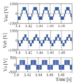
Figure 11. Line and phase voltages
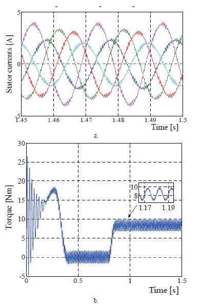
Figure 12. Five-phase motor behavior for unbalanced dc link voltages, a. stator currents, b. electromagnetic torque
The unbalancing in the line voltage are evident. The phase currents for all the five phases are illustrated in Figure 12a. The currents are shown for two cycles, to illustrate the unbalancing effect. The corresponding torque is shown in Figure 12b. Large ripple is evident in the motor generated torque, almost 25% of torque ripple is seen. This will lead to higher noise and losses in the machine.
An experimental prototype is developed in the laboratory for one cell controlled using dSpace 1006 in conjunction with FPGA board DS5203_LX. The control code is written in Matlab/Simulink and is directly interfaced to the inverter. Another four identical cells will be developed later and the results will be reported. A dc link voltage of 400V is generated. The switching frequency is kept at 5 kHz, the fundamental frequency is chosen as 50 Hz. The load connected to the inverter cell is R = 150 Ω and L = 286 mH. Level shifted carrier-based PWM technique is used similar to the simulation. The resulting waveforms are shown in Figure 13. The resulting waveform of voltage and current depicted in Figure 13, shows successful implementation of the proposed PWM. The current probe has conversion factor of 100 mV per Ampere.
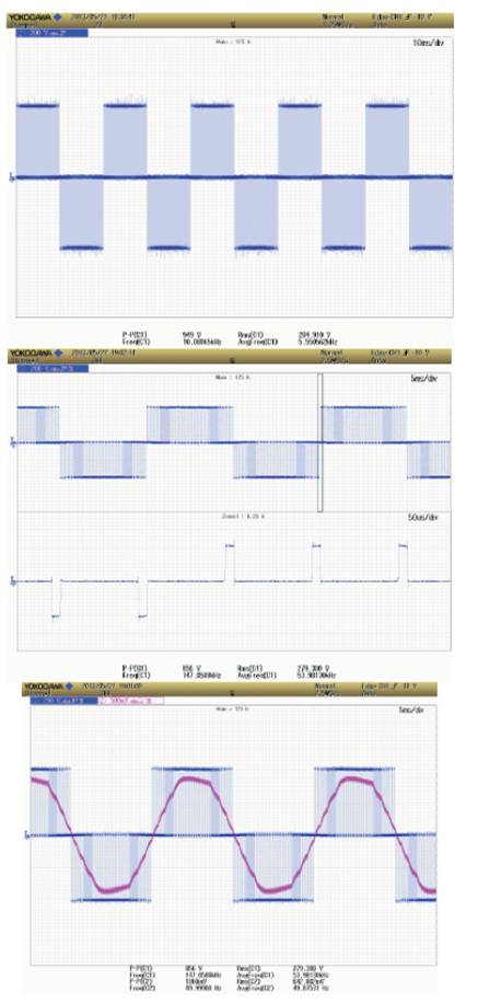
Figure 13. Experimental waveform for Cell-1
The paper discusses multi-cell three-level inverter topology for five-phase induction motor drive system. The proposed topology offer the advantages of reduced number of components when compared with the conventional topologies such as neutral point clamped and flying capacitor topologies. No clamping diodes or no clamping capacitors are needed in the proposed topologies. However, the proposed topologies requires isolated dc supplies. Another advantage of the proposed topology is the modularity, by simply adding one cell, one phase is obtained. By cascading the cells, further higher level output can be achieved. Simple level shifted sinusoidal carrier-based PWM technique is presented. Number of triangular carrier depend upon the number of level of output and in the proposed case, two carriers are needed. Simulation results are presented for balanced dc link and unbalanced DC link cases. However, experimental results are shown for just one cell that shows successful implementation.
This publication was made possible by UREP 13-41-02-17 from the Qatar National Research Fund (a member of The Qatar Foundation). The statements made herein are solely the responsibility of the authors.