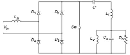
Figure 1. AC-AC Converter
An embedded controlled single-switch parallel resonant converter is introduced for induction heating applications. The circuit comprises of an input LC-filter, a bridge rectifier and a controlled power switch. The switch operates in the soft commutation mode and serves as a high frequency generator. This scheme overcomes the shortcomings of the previous schemes i.e. the presence of the DC component in the load current. The steady-state analysis of the converter is given. The theoretical analysis and computer simulation satisfy the experimental results.
Static frequency converters have been extensively applied in industry as a source of medium –frequency power supply for induction heating and melting installations. They are applied in all branches of the military, machine-building industries, jewellery making, smithy heating, domestic heating , cooking appliances and other purposes. The ordinary circuit of an AC-AC converter for induction heating, typically includes a controlled rectifier and a frequency controlled current source or a voltage source inverter. It is a well known fact that the input rectifier does not ensure a sine wave input current, and is characterized by low power[1-3]. Recently many studies of high power factor rectifiers with a single switch have been made[4-5]. These schemes are also characterized by a close to sine wave input current. Three phase AC to DC converters with improved power quality are given by [7]. A high frequency voltage fed inverter with phase shift control for induction heating is given in [8-10]. As has been shown, the converter input current is practically sinusoidal, its power factor is close to unity and the switch operates in a soft commutation regime. However, a serious disadvantage of this scheme is the presence of the DC component in the load current. It causes additional losses and rules out the possibility of using a separating transformer. The converter scheme, shown in Figure1, maintains all the advantages of the prototype, and at the same time avoids the above disadvantage. The main feature of the circuit is that the capacitor is connected in series with the load. Such a connection completely eliminates the DC component in the load current in the steady-state regime. This allows us to use the matching transformer and to apply the same converter in installations to various required levels of a load voltage. The above literature does not deal with closed loop modeling and embedded implementation of the AC to AC converter fed induction heater. In the present work, a parallel resonant AC to AC converter is modeled and it is implemented using an embedded microcontroller.
The commutation process of the proposed inverter, which consists of three time intervals, is shown in Figure 2. The idealised waveforms of the input current Iin , capacitor current IC , capacitor voltage VC , switch current Isw , the currents via the bridge diodes ID1 , ID2 and output voltage V0 are shown in Figure 3. We suppose that the switching frequency is much higher than the input line frequency, and in the analysis we arbitrarily chose the time interval where vin >0.

Figure 1. AC-AC Converter
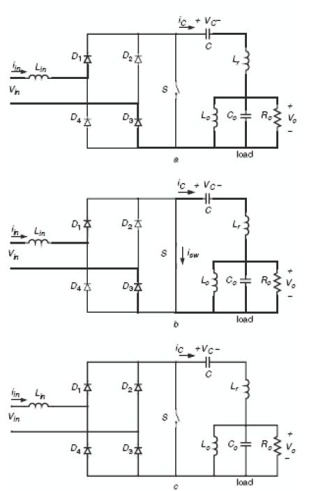
Figure 2. Equivalent Circuits Corresponding to Each Time Interval.
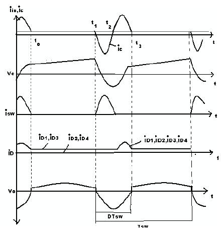
Figure 3. Ideal Switching Waveforms
The equivalent circuit is shown in Figure 2a. The switch Sw is off. The capacitor C charges up practically linearly via the circuit Lin- D1 -C-Lr load-D3.
The charge rate is determined by the instantaneous input voltage Vin .
The equivalent circuit is shown in Figure 2b. The switch Sw is on. The capacitor discharges oscillatory via the circuit Sw-C-Lr-load. The discharging current Ic varies harmonically and at the moment when the Ic reaches zero the second interval ends.
The equivalent circuit is shown in Figure 2c. Switch Sw is not in the conducting mode and the oscillatory discharging process continues via the circuit C-Lr-load-all the bridge diodes.
The analysis of the circuit operation is based on the commonly accepted assumption that all circuit components are ideal and that the capacitor discharge current can be approximated by a sinusoid. The equations are normalized using the following base quantities: base voltage VB =Vin ; base impedance RB =  Lo Co ; base current IB =VB /RB ; base power PB =VB IB ; base frequency ωB= 1/
 L0 C0 and base time
  ; here Lo, Co and Ro are the load parameters.
The maximal normalised value of the switch current is I*sw:max =Isw:max /IB =6–10 and the maximal normalized value of the switch voltage is Vsw:max =V*sw:max VB =4–5. To provide these values it is necessary to choose the following ranges of the normalised parameters: L*r =Lr /L0 =0.1_0.2; ω*r=1 Lr C /ωB =3 -5; ω*s = 1 - 2, where Lr and C are the inductance and capacitance connected in series to the load (see Figure 1).
The goal of the analytical investigation is the evaluation of the relationship between input and output voltages Mg =Vo /Vin as a function of the circuit parameters and switching frequency. This problem will be solved in three stages.
In the first stage we find the relationship between the amplitude of the capacitor current IC.max , in the first half- wave of the period, and the average value of the input current Iin , which during the switch period might be supposed as constant. Taking into account that the average capacitor current is zero, according to Figures 3 and 4,
We have
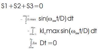
where k is the coefficient, considering the current damping in the second half-period, IC.max is the amplitude of the capacitor current, Iin is the average value of the input current, Tsw is the switching period,  is the switching frequency and D is the duty cycle. Solving (1), we obtain

In the second stage we find the relationship between the amplitude of the nth harmonic of the capacitor current lC.n.max

In the third stage we determine the relationship between the amplitude of the nth harmonic of the capacitor current IC.n.max and the amplitude of the same harmonic of the resistive component of the load current IR.n.max Obviously

with normalized quantities

where R0* = R0 /RB and ωsw = ωsw /ω
Furthermore, taking into consideration that the input and output powers are almost equal, i.e.

Thus the output-input voltage ratio is

The calculation results of the dependency of Mg by R*o and ω*sw are shown in Figure 5 (all the harmonics higher than 5th order have been neglected).
The AC to AC converter fed induction heater is simulated using the matlab simulink and the results are presented here. The open loop circuit model of the series resonant converter is shown in Figure 6a.
Scopes are connected to measure output voltage, driving pulses and capacitor voltage. The rectifier output voltage is shown in Figure 6b.
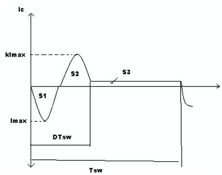
Figure 4. Determination of factor A1
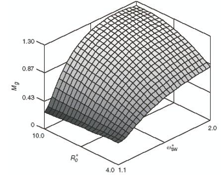
Figure 5. Factor Mg=Vo/Vin plotted against Ro* and ω*s
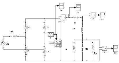
Figure 6a. Simulation Circuit
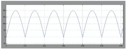
Figure 6b. Rectifier voltage
The switching pulses are shown in Figure 6c. The voltage and current waveforms of the switch are shown in Figure 6d & Figure 6e respectively. The high frequency AC output of the converter is shown in Figure 6f.
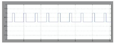
Figure 6c. Driving pulse output
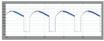
Figure 6d. Voltage across switch
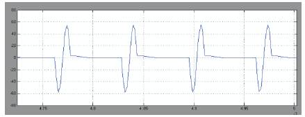
Figure 6e. Current through capacitor
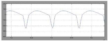
Figure 6f. Output voltage
The comparison on the performance of conventional ACAC converter and single switch AC-AC converter is presented in Table1. The results confirm that the single switch converter delivers the better performance than any other converter in achieving the better efficiency.
The ATMEL 89C2051 based control circuit is shown in Figure 6g. An ATMEL microcontroller 89C2051 was used to generate driving pulses for the MOSFET switches. They are amplified using the driver IC IR2110. The gate signal is connected to port pin P1.0.
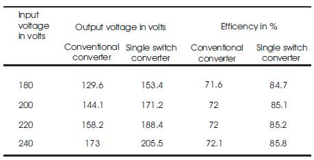
Table 1. Performance comparison
The single-switch AC-AC converter was built and tested at 230V. The experimental setup of the AC to AC converter is shown in Figure 7a. The circuit parameters are R0 =60Ω ; L0 =150μH; C0 =2.35μF; Lr=22μH; Lin =8.0mH; ωs = (62-113) x 103 s-1. The experimental waveforms of the capacitor current and output voltage at a time scale of 20 ms/div are shown in Figure 7b.
The experimental waveform of the input voltage and current are shown in Figure 7c. The output power control was also checked and it depended on the switching frequency .
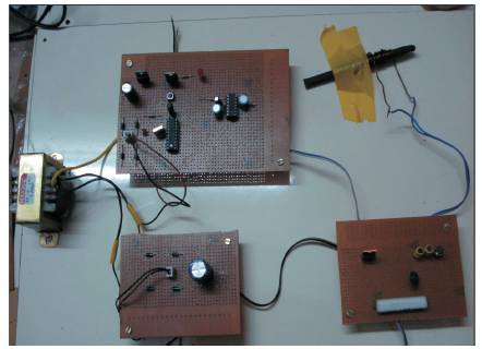
Figure 7a. Hardware layout
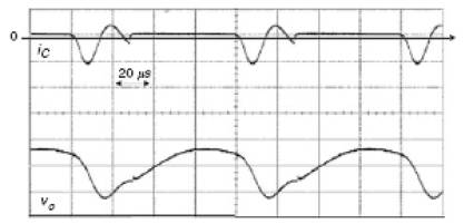
Figure 7b. Experimental waveform for capacitor current and output voltage
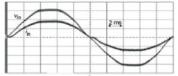
Figure 7c. Experimental waveform of input voltage and current
An embedded controlled AC-AC converter for induction heating has been presented and analysed. The basic features of the proposed circuit are as follows: (1) the converter input current is practically sinusoidal; (2) its power factor is close to unity; and (3) the output current does not include a DC-component. This prevents additional losses and allows for the possibility of using the separating transformer. The circuit topology is very simple and includes only one power switch, which operates in a soft commutation regime. The converter provides wide range power control (0.3–1). The simulation and experimental results demonstrate the actual converter capability.