(1)
Dynamic Voltage Restorer (DVR) is a custom power device used in power distribution networks to protect consumers from sudden sags and swells in grid voltage. This paper discussed abc to dq0 base new control algorithm to generate the pulse. The proposed control scheme is simple to design and has excellent voltage compensation capabilities. Effectiveness of proposed technique is investigated through computer simulation by using MATLAB/SIMULNK software. The simulation results have shown validation of the control system.
The need of the electrical power is increasing and simultaneously the problems while transmitting the power through the distribution system are also increasing. Voltage fluctuations are considered as one of the most severe power quality disturbances to be dealt with. Even a short-duration voltage fluctuation could cause a malfunction or a failure of a continuous process. There are several types of voltage fluctuations that can cause the systems to malfunction, including surges and spikes, sag, swell, harmonic distortions, and momentary disruptions. Among them, voltage sag and swell are the major powerquality problems. Voltage swell is the sudden increase of voltage to about more than 110% amplitude of the supply voltage, whereas the voltage sag is the sudden decrease of voltage ton about 90%amplitude of supply voltage. This is caused due to the sudden reduction or addition of the load across that particular feeder. This change of voltage is compensated by injecting the voltage in series with the supply from another feeder at the time of disturbances using DVR.
Electronics devices hold substantial promise for making distributed energy applications more efficient and cost effective. There is a need to develop advanced power electronics interfaces for the distributed applications with increased functionality (such as improved power quality, voltage/volt-amperes reactive (VAR) support), compatibility (such as reduced distributed energy fault contributions), and flexibility (such as operation with various distributed energy sources) while reducing overall interconnection costs. The use of voltage source inverters is increasing [1]. They are used both for feeding power from distributed generators to the transmission grid and power to various types of electronic loads. In recent years, the number of different power resources connected to power systems (voltage grids) has increased and there has been a move toward connecting small power resources to the medium and low voltage network[2].
Power quality standards for connection of an inverter to the grid are still under development, since previously there have been a few similar high power applications. In[3] it is stated that the power quality is determined by the voltage quality, when the voltage is a controlled variable. In order to deliver a good ac power the controlled pulse width modulation (PWM) inverter and L-C output filter have to convert a dc voltage source (e.g. batteries) to a sinusoidal ac voltage with low voltage THD and fast transient response under load disturbances. Another important aspect of power quality is harmonic distortion. General requirements for harmonic distortion can be found in standard [4] and particularly for connection of distributed resources to grid in [4].
PWM control is the most powerful technique that offers a simple method for control of analog systems with the processor's digital output [5]. With the availability of low cost high performance DSP chips characterized by the execution of most instructions in one instruction cycle, complicated control algorithms can be executed with fast speed, making very high sampling rate possible for digitally-controlled inverters [6]. The Z-source inverter, utilizing a unique LC network and previously forbidden shoot-through states, provides unique features, such as the ability to buck and boost voltage with a simple singlestage structure The Z-source inverter exhibits new operation modes that have not been discussed before. This analyzes these new operation modes and the associated circuit characteristics[7]. Depending upon the boosting factor capability of impedance network the rectified DC voltage is buck or boost upto the voltage level of the inverter section (not exceed to the DC bus voltage). This network also acts as a second order filter and it should be required less number of inductor and capacitor[8]. In this paper the modeling and control of voltage sag/swell compensation using new control technique based dynamic voltage restorer are simulated using MATLAB software. The simulation results are presented to show the effectiveness of the proposed control method.
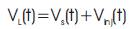
A DVR is a device that injects a dynamically controlled voltage Vinj(t) in series to the bus voltage by means of a booster transformer as depicted in Figure1. The amplitudes of the injected phase voltages are controlled such as to eliminate any detrimental effects of a bus fault to the load voltage VL(t). This means that any differential voltage caused by transient disturbances in the AC feeder will be compensated by an equivalent voltage generated by the converter and injected on the medium voltage level through the booster transformer. The DVR works independent of the type of fault or any event that happens in the system, provided that the whole system remains connected to the supply grid, i.e. the line breaker does not trip. For most practical cases, a more economical design can be achieved by only compensating the positive and negative sequence components of the voltage disturbance seen at the input of the DVR. This option is reasonable because for a typical distribution bus configuration, the zero sequence part of a disturbance will not pass through the step down transformers because of infinite impedance for this component. For most of the time the DVR has, virtually, "nothing to do," except monitoring the bus voltage. This means it does not inject any voltage (Vinj(t)= 0) independent of the load current. Therefore, it is suggested to particularly focus on the losses of a DVR during normal operation. Two specific features addressing this loss issue have been implemented in its design, which are a transformer design with low impedance, and the semiconductor devices used for switching
Mathematically expressed, the injection
Satisfies
Where VL(t) is the load voltage, Vs(t) is the sagged supply voltage and Vinj(t) is the voltage injected by the mitigation device as shown in Figure 2. Under nominal voltage conditions, the load power on each phase is given by
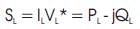
Where I is the load current, and, PL and QL are the active L L and reactive power taken by the load respectively during a sag. When the mitigation device is active and restores the voltage back to normal, the following applies to each phase
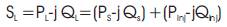
where the sag subscript refers to the sagged supply quantities. The inject subscript refers to quantities injected by the mitigation device.
The real and reactive power is given by
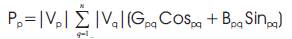
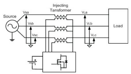
Figure 1. Schematic Diagram of DVR System
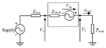
Figure 2. Equivalent circuit of DVR'
The aim of the control scheme is to maintain constant voltage magnitude at the point where a sensitive load is connected under system disturbances. The control system only measures the r.m.s voltage at the load point, i.e., no reactive power measurements are required. The proposed control scheme based on comparison of actual supply voltage and desired load voltage. The error is determined dynamically based on difference between desired and measured value. In the control scheme the actual voltage is measured and also the desired voltage. These voltages are converted in dq0 with the Parks Transformation


The control system employs abc to dqo transformation to dq0 voltages. During normal condition and symmetrical condition, the voltage will be constant and d-voltage is unity in p.u. and q-voltage is zero in p.u. but during the abnormal conditions it varies. After comparison d-voltage and q voltage with the desired voltage error d and error q is generated. This error component is converted into abc component using dq0 to abc transformation.
Phase Locked Loop (PLL) is used to generate unit sinusoidal wave in phase with main voltage. This abc components are given to generate three phase Pulses using Pulse Width Modulation (PWM) technique.
The model of proposed dynamic voltage restorer is prepared in simulink shown in Figure(3). DVR is connecting in series in the distribution system. Programmable voltage source is used as a supply voltage to simulate the voltage sag /swells. This source is responsible to generate the variation in the supply voltage. The primary side of injecting transformer is supplied by voltage sourced converter. The proposed abc to dqo converter, compares the reference voltage with actual measured voltage of DVR then accordingly generate switching pulse of voltage source converter. A virtual PLL block is used and sin-cos is given to abc to dq0 and dq0 to abc converter. The switching pulses are applied to three phase 6– pulse MOSFET based converter. The switching frequency is set on 2 kHz and sample time is 5 microseconds. The system parameters and constant value is listed in appendix
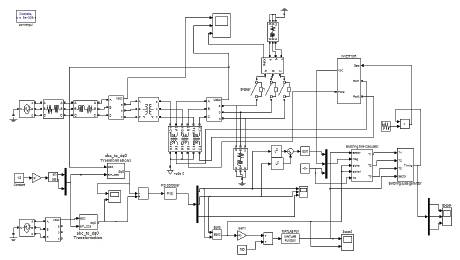
Figure 3. Overall Control Circuit of DVR Based on MATLAB Simulink
The performance of the designed DVR as shown in Figure 3 is evaluated using Matlab/Simulink. Investigation on the DVR performance can be observed through testing under various disturbances condition on the grid voltage. The proposed control algorithm was tested for balanced and unbalanced voltages sag and swells in the low voltage distribution system. In case of balance voltage sag, the source voltage has decreased about 20-25% of its nominal value. The simulation results of the balance voltage sag as shown in Figure 4. It shows the grid voltage which has dropped to0.5 p.u. (50% sag) at t=0.02 sec and the sag lasts 0.1 sec (5 cycles) and then voltage will restore back to its normal value. The function of the DVR will injects the missing voltage in order to regulate the load voltage from any disturbance due to immediate distort of source voltage. Similarly for voltage swell the waveform is shown in Figure 6. The Figure 4 and Figure 6 shows the effectiveness of the controller response to detect voltage sag and swells quickly and inject an appropriate voltage.
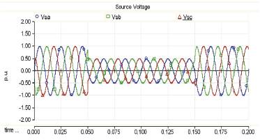
Figure 4 (a). Balanced Voltage Sag
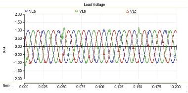
Figure 4 (b). Load Voltage After Restoration
In case of unbalance voltage swells, this phenomenon caused due to single phase to ground fault. One of the phase of voltage sag has decreased around 20-25% of its nominal value At this stage the DVR will injects the missing voltage inorder to compensate it and the voltage at the load will be protected from voltage sag problem as shown in Figure(5).

Figure5 (a). Unbalanced Voltage Sag
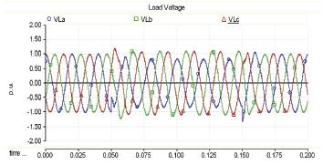
Figure5 (b). Load Voltage After Restoration
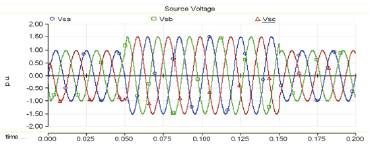
Figure 6 (a). Balanced Voltage Swell
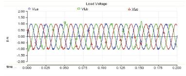
Figure 6 (b). Load Voltage After Restoration
This paper has proposed the modeling and simulation of DVR using simulink in MATLAB. The simple abc to dqo based control technique used. The performance of DVR is studied under voltage sag /swells. The ability of the DVR to compensation of voltage sag/swells has been verified. Simulation result show the DVR mitigates voltage sag /swell very fast and satisfactory in terms of voltage regulation. The DVR has effectively handled injection of proper voltage component. It can also compensate long duration voltage sag/swell.
1 Supply Voltage: Vrms = 100V
2 Series Transformer: 1:1
3 Load parameter: 100 ohm, 100 mH
4 DVR Vdc: 100 V
5 Line frequency : 50 Hz