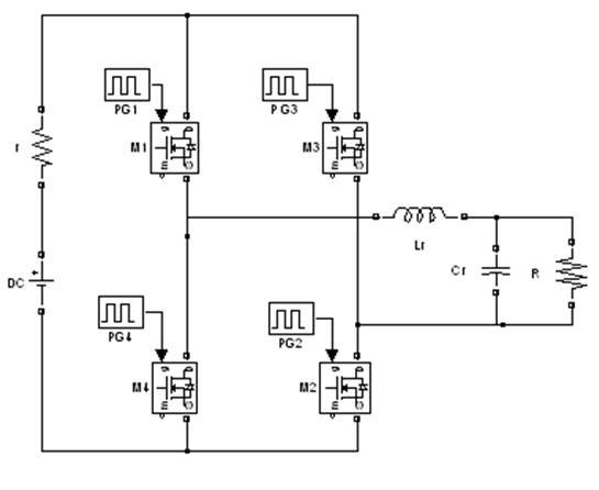
Figure 1. Basic Parallel Resonant Converter
Resonant power converters have many advantages over Pulse Width Modulation (PWM) power converters, such as lower switching losses at higher switching frequencies, easier EMI filtering, reduced component stress and higher efficiency. High switching loss considerably reduces the converter efficiency. The use of soft-switching techniques, alleviate switching loss problems and allow a significant increase in the converter switching frequency. At increased frequency the converter can employ smaller sized magnetic elements and filter components. Resonant converters eliminate most of the switching losses. The advantages of Parallel Resonant Converter (PRC) are that the output dc filter capacitor does not carry high ripple current and also it exhibits good voltage regulation. In the present work Parallel Resonant Converter (PRC) with Zero Voltage Switching (ZVS) for the 12 V DC output is designed with High Frequency (HF) and the simulation results are presented.
The characteristics of the parallel resonant converter are quite different from those of the series resonant converter, and from those of conventional PWM converters. The parallel topology can both step up and step down the dc voltage. Although the output characteristics are again elliptical, near resonance they exhibit a current-source characteristic. The discontinuous conduction mode occurs under heavy loading (or short-circuit conditions, in the limit). The transistor current stresses and conduction loss depend on the output voltage, and are nearly independent of load current.
Resonant converters can be operated with much higher frequency without increasing switching losses, and leakage inductances of HF transformer are being used advantageously as part of resonant inductances. They are particularly useful for the applications like telecommunications, where higher input voltages are used. ( Hamed S et al 2011). Recently, developments in resonant converters are shifting towards high order resonant converters in which the tank circuit has more than two reactive components ( M.-C. Tsai, 1991). The growing demand for smaller, lighter and efficient power converters led into a great research effort to increase the operating frequency of power converters without reducing its efficiency ( Nuno Filipe Pereira, 1996).
To meet the ever increasing demand of miniaturizing power supplies in high-tech equipments, it becomes necessary to use high-frequency switching converters. But with the PWM technique, high-frequency switching has many disadvantages such as high switching losses and stresses, low efficiency, increased Electro-Magnetic Interference (EMI) problem, and poor reliability. These deficiencies can be greatly reduced with resonant converters which have sinusoidal waveforms often switched at low di/dt and/or dv/dt. Hence, the switching losses in the power switches, the rectifier diodes are greatly reduced so that the operation at high frequencies is possible with increased efficiency and reliability. Due to the waveform nature of the resonant circuits, the stresses in the switching components are reduced with easier EMI filtering and decreased noise problems. ( Marian K. Kazimierczuk and Manikantan K. Jutty,1995).
Based on the converter topology, resonant converters may be classified according to the methods of coupling between the resonant and the output circuits. In general, we may classify them into two types: the resonant and the non-resonant coupling. In the resonant coupling, the resonant circuit is used to buffer and transfer energy from the source to the load. The effect of output loading in this case is manifested itself by changing the DC levels of resonant voltage and/or current waveforms. The conventional parallel and series resonant converters with inductive and capacitive output filters, respectively, are typical examples of resonant coupling. However, in the case of non-resonant coupling, the output circuit is completely decoupled from the resonant circuit, when the converter is resonanting at its natural frequency. The parallel resonant converter with capacitive output filter is an example of such converters. ( S. Sooksatra and C.Q. Lee, 1989).
Resonant transition converters are characterized by low switching losses and low conduction losses ( B.Swaminathan and V.Ramanarayanan, 2004). Although LLC series resonant converter has advantages of wide operation range and high efficiency, hold up time requirement makes it difficult to optimal design at normal operating condition, results in increasing transformer size and low efficiency ( Bong-Chul Kim et al, 2009). The analysis, design and control of fourth-order LCLC voltage-output series-parallel resonant converters for the provision of multiple regulated outputs was given by Christopher M. Bingham (2008). Magnetizing current of transformer is included in primary winding of the transformer, it can't be used to generate the driving signals of SRs directly ( Xinke Wu et al, 2010).
Resonant inverters can be realized with thyristor switches, because the resonant load can be used to commutate the thyristor. In order to achieve effective commutation, the load must be driven at a frequency such that a leading power factor is presented to the inverter. The operating frequency in a thyristor inverter can not be sufficiently high, because of its high turn-off time. Consequently in modern DC to DC converters, high frequency high power switching devices such as BJT, IGBT or power MOSFETs are used. Here we are using MOSFETs.
A parallel resonant full bridge inverter is used for the investigation is presented in Figure 1. The circuit consists of full bridge MOSFET inverter. The resonant inductor Lr and capacitor Cr. The resonant capacitor is in parallel with the load and they form a Parallel LC circuit. From this configuration, the resonant tank and the load circuit act as a voltage divider. By changing the frequency of the input voltage, the impedance of the tank will change. This impedance will drive the input voltage with the load. At resonant frequency, the impedance of parallel resonant tank will be very high.
Figure 1. Basic Parallel Resonant Converter
Figure 2 shows the equivalent circuit for parallel resonant converter. Let the inverter AC output voltage being VRms and the load side voltage be VRac. From the equivalent circuit the voltage transfer function is given by,
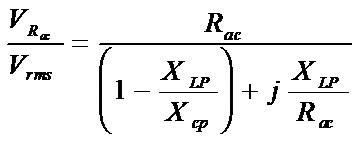
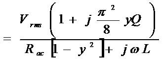
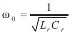
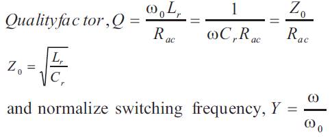

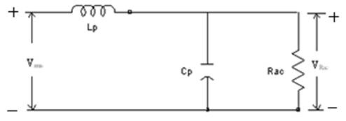
Figure 2. Equivalent circuit for parallel loaded resonant converter.
Figure 3 shows the simulation circuit for full bridge parallel resonant converter. The circuit consists of a AC input source, full bridge diode rectifier, filter circuit, full bridge MOSFET inverter having a HF resonant circuit. A HF transformer provides voltage transformation and isolation between the source and the load. A load can be connected to the high frequency link circuit with secondary rectifier and smoothing capacitor.
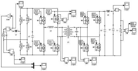
Figure 3. Simulation Circuit for Full Bridge Parallel Resonant Converter
The input AC source is rectified by full bridge diode rectifier. The rectified DC voltage is filtered by using capacitor. The DC voltage is inverted by high frequency MOSFET full bridge inverter. Pulse generators are connected to the gate of the MOSFET. Output of the inverter is connected to primary of the transformer through resonant inductor. When M1 M4 conducts, M2 M3 should be in off state and vice versa, to avoid short circuit. When the MOSFET M1M4 conducts, the current flows through MOSFET M1, resonant inductor L, transformer primary and MOSFET M4. The resonant current flows in clock wise direction. When the MOSFET M2M3 conducts, the current flows through MOSFET M2, transformer primary, resonant inductor L and MOSFET M4. The resonant current flows in anti-clock wise direction. The secondary of the transformer is then connected to MOSFET full bridge rectifier. The resonant capacitor is connected in secondary instead of primary. The LC tank circuit is called as resonant circuit.
The resonant link circuit is driven with either square waves of voltage or current in the inverter. The voltage or current in the resonant components becomes minimum at the resonant frequency and by altering the frequency around the resonant point, the voltage on the resonant components can be adjusted to any desired value. By rectifying the voltage across the secondary of the transformer, a DC voltage is obtained which is filtered to achieve smooth DC. Scopes are connected to display the input current and voltage, gate pulses, output voltage, current, etc.
The simulation of full bridge parallel resonant converter is done using Matlab and results are presented. Figure4 shows the driving pulse for MOSFET M1 and M2. When the pulse to MOSFET M1 & M4 is high the pulse to MOSFET M2 & M3 must be low to avoid short circuit.
Figure 5 shows the driving pulse for MOSFET M1 and Drain to source voltage of MOSFET M1. From the wave form it is clear that when the pulse to the MOSFET is high the output is low. (ie) the switch is conduction state. When the device conducts, the voltage across the device is very less.
DC output voltage wave form is shown in Figure 6. The value of output is 12V. DC output current is shown in Figure. 7. Its steady current is 0.14 A. Output power waveform is shown in Figure 8.
Figure 9 shows the source voltage and source current waveforms. From the graph it is clear that when the voltage attains maximum value, the current also attains maximum value at the same time. The voltage and current waveforms are in phase with each other. The phase angle between voltage and current is very small. Results in improved power factor. Under resonant condition the capacitive reactance are equal to inductive reactance, and the circuit is said to be pure resistance, the power factor is nearly unity.
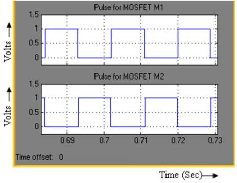
Figure 4. Driving Pulse for MOSFET M1 and M2
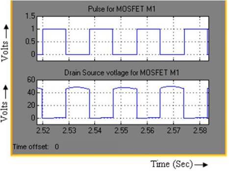
Figure 5. Driving Pulse for MOSFET M1 and Voltage across MOSFET M1
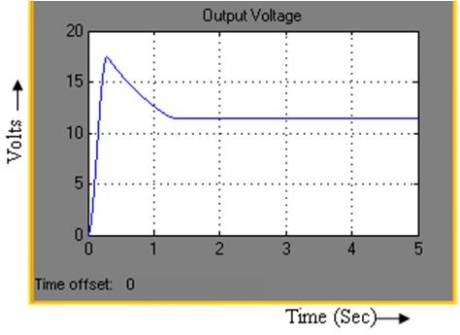
Figure 6. Output Voltage
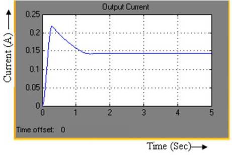
Figure 7. Output Current
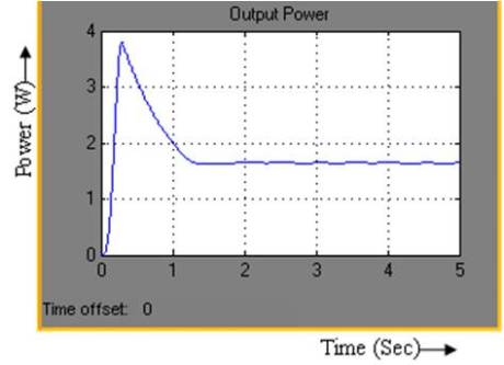
Figure 8. Output power
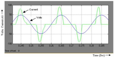
Figure 9. Input Voltage and Current waveforms
Parallel resonant full bridge DC-DC converter is simulated using Matlab simulink and the results are presented. The results shows that the output voltage is smooth and the ripples are reduced. There by increasing the switching frequency, the switching loss and voltage stress on the switch is reduced. The efficiency of the converter is improved. The parallel resonant converter has the advantages like high power density, reduced EMI, reduced switching losses and stresses with improved power factor. AC to DC power supplies with 12 V DC has many industrial applications such as Aerospace, Military, Rail & Automotive, Medical, Telecom networking, etc.