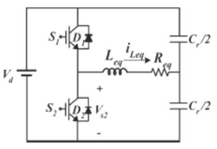
Figure 1. Class-D Inverter System
This paper deals with digital simulation of Class D and Class E inverter fed induction heater system. This system has an advantage like reduced volume and switching losses. The circuit operates under zero voltage switching. The circuit models of Class D and Class E are developed and they are used for simulation studies. The simulation results are compared and results are presented.
Induction Heating was first noted when it was found that heat was produced in transformer and motor windings. Accordingly, the theory of induction heating was studied so that motors and transformers could be built for maximum efficiency by minimizing heating losses. The development of high-frequency induction power supplies provided a means of using induction heating for surface hardening. The early use of induction involved trial and error with built-up personal knowledge of specific applications, but a lack of understanding of the basic principles. Throughout the years the understanding of the basic principles has been expanded extending currently into computer modeling of heating applications and processes. Knowledge of these basic theories of induction heating helps to understand the application of induction heating as applied to induction heat treating. Induction heating occurs due to electromagnetic force fields producing an electrical current in a part. The parts heat due to the resistance to the flow of this electric current.
A high-frequency class-D/Class E inverter has become very popular and is more and more widely used in various applications. It must be effectively selected according to the applications in order to meet the inverter requirements under a high-frequency switching operation due to load specifications. In addition, one of the main advantages of the class-D inverter is low voltage across the switch, which is equal to the supply voltage. Thus, compared with other topologies (class-E quasi-resonant inverter, etc.) for IH applications [2], the class-D/Class-E inverter is suited for high-voltage applications [1], [4]. Generally, almost all IH applications use a variable-frequency scheme, pulsefrequency modulation (PFM), and pulse-amplitude modulation (PAM) to control the output power [3], [5], [6]. Between them, frequency modulation control is the basic method that is applied against the variation of load or line frequency.. Additionally, in case of operation below resonance, filter components are large because they have to be designed for the low-frequency range. In addition, it is apt to audible noise when two or more inverters are operated at the same time with different switching frequencies. Besides, the soft-switching operating area of the zero-voltage switching (ZVS)–PFM high-frequency inverter is relatively narrow under a PFM strategy [8], [9], [10].Keeping the constant switching frequency and controlling the output power by pulse width modulation (PWM) are obvious ways to solve the problems of variable-frequency control. Therefore, class- D-inverter topologies using a PWM chopper at the input, phase-shifted PWM control, PWM technique, pulse width modulation–frequency modulation(PWM–FM) technique, current-mode control, and a variable resonant inductor or capacitor have been proposed [7]–[11], [12]. The constant-switching-frequency operation supposes that each inverter in the applications is operating at the same frequency, making it necessary to control power without frequency variations, and this is highly desired for the optimum design of the output smoothing and noise filters. However, these control requirements and operating characteristics have considerable complexity due to the fixed switching frequency, which limits their performance [12]. In addition, if the system is operated with phase-shifted PWM control, the ZVS is not achieved at light load [13], [14]. To simplify output-power control, a full bridge zero-current switching (ZCS)–pulse-density modulation (PDM) class-D inverter is proposed [15]. The output power of the ZCS–PDM class-D inverter can be controlled by adjusting the pulse density of the square-wave voltage. However, when the output is controlled by the pulse density, like that in [15], [16], the load current should be freewheeled, and then, the output voltage of the inverter becomes zero. As a result, the conduction losses of the inverter are caused by the freewheeling current during the freewheeling mode. Therefore, to solve these problems, this paper deals with a simple power-control scheme of constant frequency variable power (CFVP) for the class-D inverter in the IH-jar application without additional devices. When the class-D inverter operates at a fixed switching frequency that is higher than its resonant frequency, it can maintain ZVS operation in the whole load range. Thus, the switching losses and electromagnetic interference (EMI) are decreased. In addition, by adjusting the duty cycle of fixed low frequency, the output power is simply controlled in a wide load and line range. The advantages of a new power-control scheme are simple configuration and wide power-regulation range. It is easy to control the output power for wide load variation. In addition, the switches always guarantee ZVS from light to full loads, and a filter is easy to design by using the constant switching frequency. The proposed power-control scheme and principles of the class-D inverter are explained in detail. The theoretical analysis, simulation, and experimental results verify the validity of the class-D inverter with the proposed powercontrol scheme.
A class-D inverter will be generally used to energize the induction coil to generate high-frequency magnetic induction between the coil and the cooking vessel, consequently, high-frequency eddy current and heat in the vessel bottom area. The class-D inverter takes the energy from the input source. The DC voltage is converted again into a high-frequency AC voltage by the class-D inverter. Then, the inverter supplies a high-frequency current to the induction coil. Figure 1 shows the class-D inverter system of IH jar. The class-D inverter consists of two switches S1 and S2 with antiparallel diodes D1 and D2 , two resonant capacitors Cr/2, and an induction coil that consists of a series combination of equivalent resistance Req and inductance Leq.
The DC input voltage is directly supplied into an inverter. Then, (S1, D1 ), and (S2 , D2 ) are alternately used to administer a high-frequency current to the induction coil. Figure. 2 represents the equivalent circuit model of the class-D inverter. In particular, two switches are operated at square wave with suitable dead time between the two driving commands. The class-D inverter is operated above the resonant frequency, which means that the switches are turned on with ZVS.
Figure 1. Class-D Inverter System
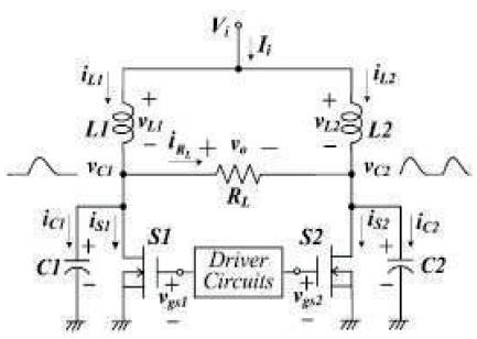
Figure 2. Basic Push Pull Class- E Power Amplifier
The basic schematic of the proposed push–pull Class-E series- parallel LCR resonant PA is shown in Figure 2. It contains two MOSFETs, two inductors, two capacitors, and a load resistance.
Switches S1 and S2 are complementarily activated to drive periodically at the operating frequency f = ω/2π as in a push–pull switching PA[10],[11],[13], i.e., the switch waveforms are identical, except that the phase shifts between S1 and S2 are with an “on” duty ratio D of less than 50%. The simplest type of half-amplifier is a seriesparallel resonant circuit, which consists of an inductor L in series with a paralleled capacitor C and resistor R. The resistor RL is the load to which the AC power is to be delivered, with neither end connected to a ground. It is suitable for a load that is balanced to a ground, but most RF-power loads have one end connected to a ground. To accommodate grounded loads, the proposed topology needs to add one of the following: a balun that can be used to provide the interface with the amplifier [14-15]; or a two-winding transformer (that has Vi connected to a center-tap on the primary winding), between the grounded load (on the grounded secondary winding) and the drains of S1 and S2 (connected to the ends of the center-tapped primary winding). To reduce the transistor turn-on power losses, the switch current is increase gradually from zero after the switch is closed. The proposed push–pull Class-E PA [16] uses a pair of LC resonant networks with an overlapped capacitor-voltage waveform; this offers additional degrees of freedom.
Class D/E inverter systems are simulated and the results are presented here. Class D inverter circuit is as shown in Figure 3.a. Scopes are connected to measure the voltages. Class D Inverter DC input voltage is shown in Figure 3.b. and its output voltage is as shown in Figure 3.c. Similarly Class E inverter circuit is shown in Figure 4.a. DC input voltage is shown in Figure.4.b. Class E inverter output voltage is as shown in Figure.4.c. Comparisons of Input Voltage vs Output Voltage & Input Voltage vs Output Power are as shown in Figures 5 & 6. respectively.
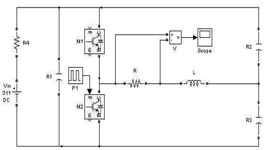
Figure 3(a). Class D circuit Diagram
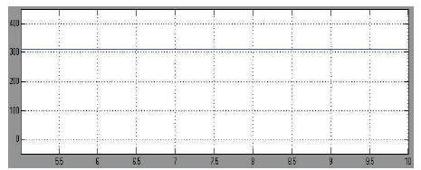
Figure 3(b).Input D.C Voltage
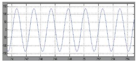
Figure 3(c). Output Voltage
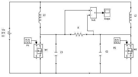
Figure 4(a). Class E Circuit Diagram
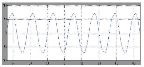
Figure 4( b). Output Voltage
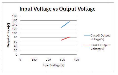
Figure 5. Input Voltage vs Output Voltage
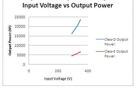
Figure 6. Input Voltage vs Output Power
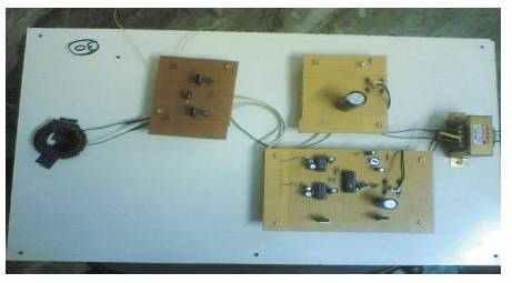
Figure 7(a). Top View of the Hardware

Figure 7(b). Dc Input Voltage
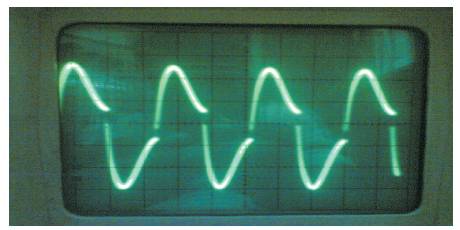
Figure 7( c) Output of the Inverter
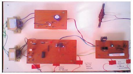
Figure 8(a). Top View of the Hardware
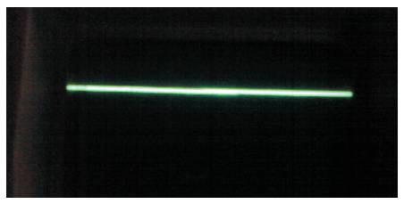
Figure 8.b. DC Input Voltage
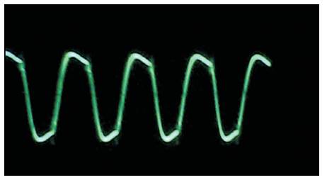
Figure 8.c. Output Voltage of the Inverter
Laboratory model for class D inverter is fabricated and tested. Top view of the hardware is shown in Figure 7.a. The hardware consist of control board and power board. The pulses are generated using microcontroller. DC input voltage is shown in Figure 7b. Output of the inverter is shown in Figure 7c. Output is not a pure sine wave due to the resistance present in the circuit.
The laboratory model for class E inverter fed induction heater is fabricated and tested. Top view of the hardware is shown in Figure 8a. The hardware consists of power circuit and control circuit. DC input voltage is shown in Figure 8b. Output voltage of the inverter is shown in Figure 8.c. The output is not a pure sine wave due to the resistance of the coil.
A Class D/Class E inverter fed induction heater is studied and simulated using Matlab Simulink. The comparisons of simulation results are presented. It is observed that
Also this class D system operates at high efficiency due to soft switching. This system has advantages like reduced volume, and faster response. Volume of L and C is reduced due to high frequency operation. Hardware is reduced since it uses only two switches. Faster response is obtained by using Atmel micro controller. The simulation results are in line with predictions. This work deals with simulation studies and Hardware implementation. The experimental results are in line with the simulation results.
The authors are acknowledge the support given by Power Electronics division, in Bharath University, and Ganadipathy Tulsis Jain Engg College for conducting the simulation studies during May 2011 to June 2011.