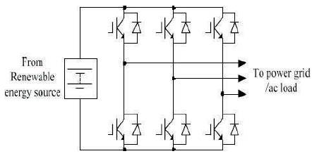
Figure 1. Configuration using a single PWM inverter.
With the increased compulsory usage of renewable energy resources, it is essential to efficiently use the energy produced from them. Such energy can be stored in fuel cells which work on the basis of electrolysis. A DC-DC converter is required to couple the electrolyser to the system DC bus. This paper is based on a new approach for achieving very high conversion efficiency in low-voltage high-power isolated boost DC-DC converter. The proposed DC-DC converter is realized in half-bridge topology in the rectifier side to achieve zero voltage switching for the power switches and to regulate the output voltage. Z-Source inverter is utilized to realize inversion and boost function in one single stage. In this DC-DC Converter the winding losses and the switch conduction losses are reduced. The transformer eddy-current and proximity effects are analyzed. The MATLAB simulation results show that the output of converter is free from the ripples and regulate the output voltage. The experimental results are verified to validate the simulation results. The ability to boost and buck voltage makes the Z-Source inverter very attractive for electrolyser application.
Renewable energy includes solar energy (photovoltaic, PV) [1-2], wind energy, bio-fuel, geothermal energy, hydrogen and fuel cells, etc. These energy sources are renewable and utilization of these energy sources creates zero or little if any emissions. Furthermore, Distributed Generation [3-4](DG) systems using renewable energy have great potential to increase the grid reliability. Currently, renewable energy systems are still relatively expensive and therefore the cost, $/kWh, is higher than using fossil fuel. For this reason, renewable energy sources have captured only a small share of the total energy market. However, with the continued development of technology, the cost of photovoltaic cells is decreasing steadily and it will become as or more cost effective. Therefore, one can foresee a large future market for PV systems. However, for renewable energy DG, the demanded output voltage of the system is constant and 50/60 Hz ac regardless of the output voltage of the energy sources. All the existing power conversion topologies used in today's PCS or utility interface can be boiled down to two basic circuits as shown in Figures. 1 and 2.
To efficiently use PV systems, power electronics is essential. Sometimes, they are the most expensive part of the power generation system. Reducing cost, increasing efficiency, and improving reliability of power electronics and electric machines are the technical challenges facing wider implementation of PV power generation. Electrolyser is a part of renewable energy system ,it generates hydrogen from water electrolysis that is used in fuel cells. Owing to this scenario, this paper is directed towards the design of a novel Z-source isolated boost DC-DC converter for electrolyser application.
Figure 1. Configuration using a single PWM inverter.
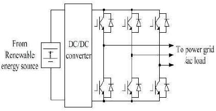
Figure 2. Configuration using a DC-DC converter and a PWM inverter.
History of the Electric Automobile has been done by E.H.Wakefield in Warrendale 1998[1]. Microcontroller-based, photovoltaic maximum power point tracking control system has been done by E.Koutroulis, K.Kalaitzakis and N.C. Voulgaris in 2001[2]. Design of Z-Source Inverter has been done by Fang Zheng Peng in 2003[3]. Maximum constant boost control of the Z source inverter has been done by Miaosen Shen, Jin Wang, Alan Joseph, Fang Z. Peng, Leon M. Tolbert, and Donald J. Adams in 2004[4]. Comparison of traditional inverters and Z-Source inverter has been done by Shen, M.; Joseph, A.; Wang, J.; Peng, F.Z.;Adams, D.J. in June 2005[6]. Z-source inverter control for traction drive of fuel cell - battery hybrid vehicles has been done by Kent Holland, Miaosen Shen, Fang Z. Peng Oct 2005[7]. A Z-Source Inverter for Residential Photovoltaic Systems has been done by Y. Huang; M. Shen; F. Z. Peng; J. Wang in 2006[8]. Current-fed dual-bridge DC–DC converter has been done by W. Song and B. Lehman in 2007.A ZVS bidirectional DC–DC converter with phase shift plus PWM control scheme has been done by H. Xiao and S. Xie in 2008[10]. High-efficient fuel cell power conditioning system with input current ripple reduction has been done by J.-M. Kwon, E.-H. Kim, B.-H. Kwon, and K.-H. Nam in 2009[11]. High- Efficiency Isolated Boost DC-DC Converter for High-Power Low-Voltage Fuel-Cell Applications has been done by Morten and Michael A.E. Andersen in 2010[12]. An attempt has been made in the present work to implement the Zsource Isolated Boost DC-DC Converter for Electrolyser Application Using Renewable Energy.
In renewable energy systems, the main challenge is the output voltage variation of the energy source. The ability to boost and buck voltage makes the Z-Source inverter very attractive for electrolyser application.
Z-Source inverter [2] is utilized to realize inversion and boost function in one single stage. With a unique impedance network of inductors and capacitors, the Z-Source inverter utilizes [5] the shoot through states by gating on both the upper and lower switches in the same phase legs, to boost the DC voltage without DC/DC converter. The shootthrough states are forbidden in the traditional voltage source inverter. The Z-Source shows more reliability in applications because of its ability of handling shootthrough states. The inductors and capacitors can be optimally designed to lower the cost and size.
Compared with the traditional systems, the[6] Z-Source PCs does not need bulky transformers or DC-DC converter to boost the voltage in the circuit. Usually transformerless inverter can gain 2-3% in conversion efficiency. The switch in the DC-DC converter will make the efficiency lower and the cost higher. Thus for the Z-Source inverter system, the size and cost are minimized. Because no dead time is needed, the control accuracy and harmonics can also be improved. The Z-Source inverter can have the minimum KVA requirement to meet the need of 1:2 output voltage ranges for most renewable energy sources.
To verify some features of the Z-Sources inverter for renewable energy sources, a Z-Source inverter for PV residential systems [8]. is considered. If a traditional inverter system is used to produce a +/-120 V split-phase power, the minimum dc voltage is 340-680 V with a PV voltage change range of 1:2. Given a 10 KW PV system, a 20 kW inverter is needed to cope with the voltage change and 1200 V c have to be used. Using the Z-source inverter system, the PV voltage can be designed to be 225-450 V, which can be boosted and inverted to +/-120 V splitphase power by the Z-Source inverter using 600 V MOSFET s instead of the 1200 V MOSFET s needed in the traditional system. In addition, the required KVA rating of the Z-Source inverter remains 10 KVA, half of that of the traditional voltage source inverter system. In addition, the Z-source system is able to provide maximum power tracking and voltage boost simultaneously and independently by one single inverter.
There are two basic operation modes of the Z-Source inverter to the Z-Source network: shoot-through mode and non-shoot through mode (or any traditional inverter switching state). The relationship among the boost factor (B), shoot through duty cycle (To/T), capacitor voltage (Vc1, Vc2), and output peak voltage (Vac) are Figures. 3 and 4 Equivalent Circuit when ZSI in shoot & non shoot-through State.
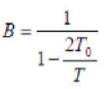
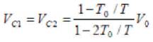
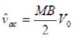
Where M is the modulation index, T is the switching period, and To is the shoot-through interval.
There are four control methods that have been developed for the Z-Source inverter: simple boost, maximum boost, maximum constant boost, and modified PWM. Figure 5 shows the simple boost control method for the Z-Source inverter system Figures 3 & 4 where two straight lines are used to control the shoot through intervals. As shown in Figure 5, the circuit is turned into shoot through states by gating on all switches when the carrier is greater than the upper line or lower than the bottom line.
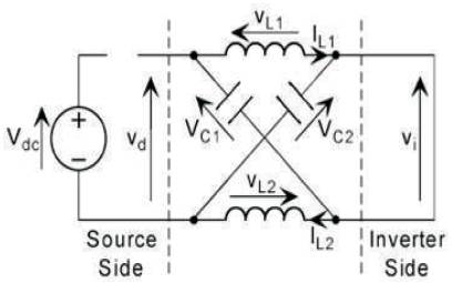
Figure 3.Equivalent circuit when ZSI in shoot through state
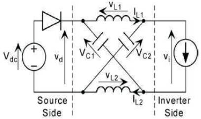
Figure 4 .Equivalent circuit when ZSI in non shoot through state
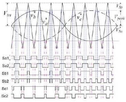
Figure 5. The Simple Boost Control Waveforms for Z-Source Inverter
High-power fuel-cell or battery-powered applications, such as for transportation, forklift trucks, or distributed generation, are often faced with the need for boosting the low input voltage (30–60 V) to the much higher link voltage (360–400 V) required for interfacing to the utility grid.
For safety and electromagnetic compatibility reasons, galvanic isolation between source and utility grid is often required. In a 400-V output application, 600-V rated diodes will be sufficient in boost-type topologies. But, buck-derived topologies require 1200-V diodes or stacking of multiple outputs. Moreover, clamp circuits will be required across rectifier diodes in buck-derived topologies.
Isolated boost converters have some inherent advantages when used in fuel-cell applications [12].. Boost-type topology is the need for the clamping of voltage spikes on primary switches caused by parasitic inductances. Buck-type topology have inherently larger rectifying losses than boost type topologies. A very high efficiency in low-voltage high-power Z-Source isolated boost DC-DC converters [9] has been proposed in Figure 6. The over sizing of the primary-switch voltage rating can be avoided, significantly by reducing switch conduction losses. Z-Source is used to boost or buck the voltage and also improve the performance of the converter [10,11]. ZSource inverter has more reliable due to shoot through capability. High-power fuel-cell or battery-powered converter is shown in Figure 7 which is mostly used in transportation, forklift trucks and distributed generation with interface to grid system.
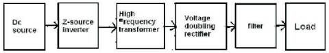
Figure 6. Basic Block Diagram Z-Source Isolated Boost DC-DC Converter
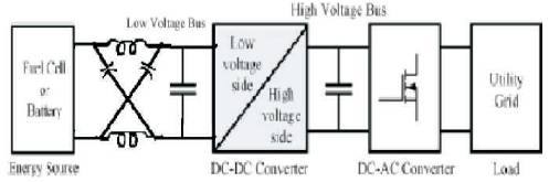
Figure 7. Fuel-cell Z-Source Power System with Isolated High-Gain DC-DC Converter.
Primary switches S1-S4 are hard switched and operated in pairs, i.e., S1 –S2 and S3 –S4 , respectively Shown in Figure 8. The drive signals are 180 phase shifted. Switch-transistor duty cycle D is above 50% to ensure switch overlap and, thus, a continuous current path for the inductor L1 current.
The energy transfer to output starts when switches S3 and S4 are turned off. Inductor current IL1 flows through primary switch S1 , transformer T1 , rectifier diode D1 , and output capacitor C1 and returns to input through primary switch S2 . Inductor current IL1 discharges. The period ends when primary switches S3 and S4 are turned on again.
During switch overlap, when all switches S1 –S4 are turned on, the inductor current IL1 is charged is Shown in Figure 9. The current in the transformer secondary winding is zero, and diodes D1 and D2 are off. The transformer magnetizing current circulates in the transformer primary winding through switches S2 –S4 and/or S1 –S3 . Capacitors C1 and C2 supply the load current. The period ends when primary switches S1 and S2 are turned off.
A second energy-transfer cycle starts when switches S1 and S2 are turned off and ends when S1 and S2 are turned on again. The inductor current IL1 flows through switches S3, T1, D2, and C2 and returns to input through S4 .
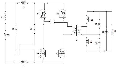
Figure 8. Circuit diagram Z-Source Isolated Boost DC-DC Converter
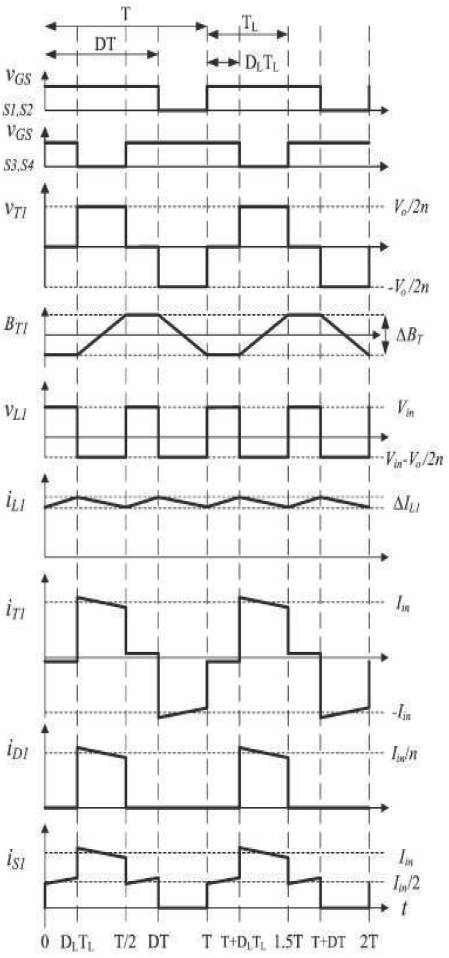
Figure 9. Basic Operating Waveforms of Isolated Full-bridge Boost Converter
The simulation is done using MATLAB simulink and results are presented. Scope is connected to display the output voltage. Figure 10. shows Z-source based full -bridge converter with voltage doubling rectifier. Figure 11 shows DC input voltage waveform. Figure. 12. Shows M4 Gate pulse and drain to source voltage waveform (Vg & Vds). Figure. 13 shows M2 Gate pulse and drain to source voltage waveform (Vg & Vds). Figure. 14 shows Voltage across VL1. Figure 15 shows Transformer primary voltage waveform (Vp). Figure 16 shows Transformer Primary current waveform (iL1). Figure 17. shows Transformer secondary voltage waveform (Vs). Figure 18 shows Output current waveform. Figure 19 shows Output voltage waveform. Figure 20 shows Output power waveform. Figure 21shows Input voltage Vs Output voltage. Figure 22 shows Input voltage Vs Output power. Figure 23. shows Output power Vs Efficiency
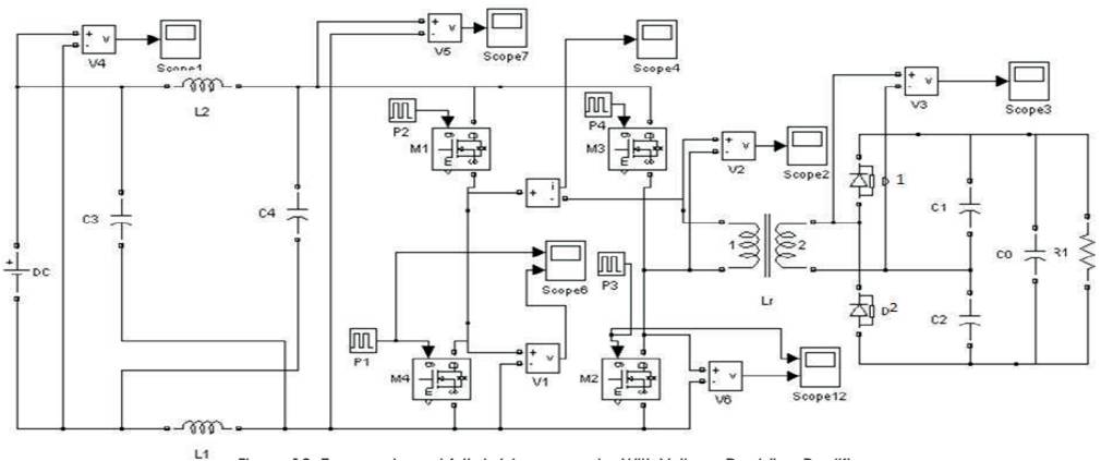
Figure 10. Z-source based full –bridge converter With Voltage Doubling Rectifier
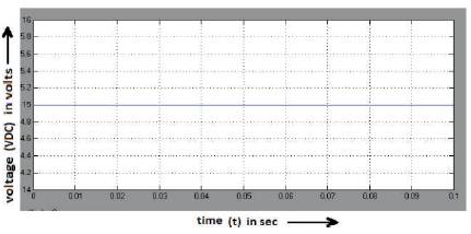
Figure 11. DC Input Voltage Waveform
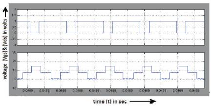
Figure 12. M4 Gate pulse and drain to Source Voltage Waveform (Vg & Vds)
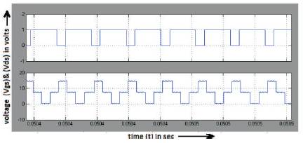
Figure 13. M2 Gate pulse and drain to Source Voltage Waveform (Vg & Vds)
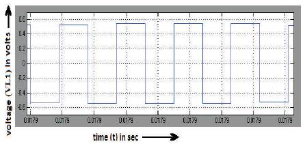
Figure 14. Voltage Across VL1
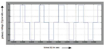
Figure 15. Transformer Primary Voltage Waveform (Vp)
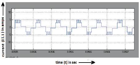
Figure 16. Transformer Primary Current Waveform (iL1)

Figure 17. Transformer Secondary Voltage Waveform (Vs)
Figure 18. Output Current Waveform
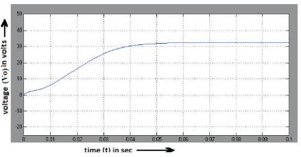
Figure 19. Output Voltage Waveform
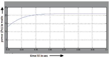
Figure 20. Output Power Waveform
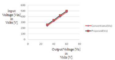
Figure 21. Input voltage Vs Output voltage
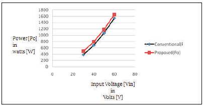
Figure 22. Input voltage Vs Output power
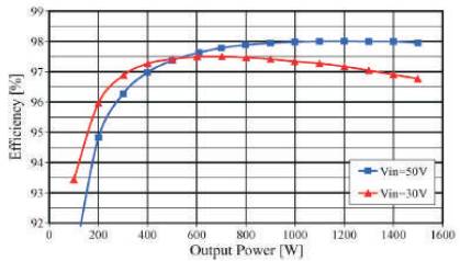
Figure 23. Output power Vs Efficiency
The hardware is fabricated and tested in the laboratory. Pulses required by the MOSFETs are generated by using a microcontroller. These pulses are amplified by using a driver amplifier. Figure 24 shows the hardware layout. Figure 25 shows the Input Voltage is Measured Using Multimeter. Figure 26 shows the Control circuit for generating the driving pulses. Figure 27 shows the DC Input Voltage. Figure 28. shows the Triggering pulse. Figure 29 shows the Gate pulse and Drain to Source Voltage Waveform (Vgs & Vds). Figure. 30 shows the Transformer Primary Voltage waveform (Vp). Figure 31 shows the Transformer Secondary Voltage Waveform (Vs). Figure. 32. shows the Output Voltage is Measured Using Multimeter.
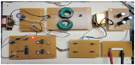
Figure 24. Hardware layout
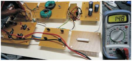
Figure 25. Input Voltage is Measured Using Multimeter
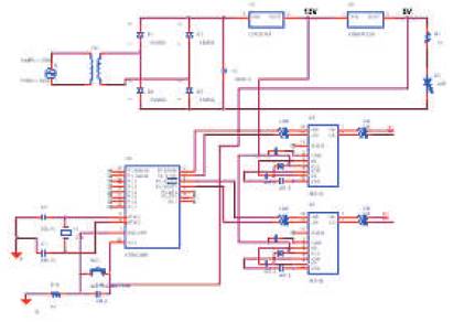
Figure 26. Control circuit for Generating the Driving Pulses
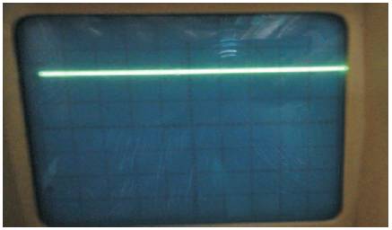
Figure 27. DC Input Voltage
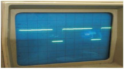
Figure 28. Triggering Pulse
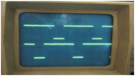
Figure 29. Gate pulse and Drain to Source Voltage Waveform (Vgs & Vds)

Figure 30. Transformer Primary Voltage waveform(Vp)
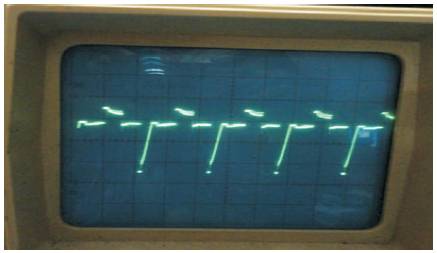
Figure 31. Transformer Secondary Voltage Waveform (Vs)
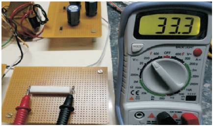
Figure 32. Output Voltage is Measured Using Multimeter
A Z-source Isolated Boost DC-DC Converter is simulated and experimentally tested in the laboratory. The proposed DC-DC Converter achieves very high efficiency in lowvoltage high-power isolated boost DC-DC converter. High-power low-voltage transformers require an extensive interleaving of windings to keep AC resistances low. Extremely low primar y leakage inductances are achieved, allowing the dissipation of stored leakage energy. Thus, the voltage rating of switches rated for unclamped inductive switching can be reduced, greatly improving converter efficiency to 98%. The proposed converter has advantages like fast current switching, low parasitic circuit inductance, very high efficiency ,reduced Switching losses, reduced switching stresses, reduced EMI increased power density and high efficiency. Thus, the voltage rating of the switches rated for unclamped inductive switching can be reduced, greatly improving converter efficiency. Power density is increased by increasing the frequency which in turn reduces the frequency. The ability to boost and buck voltage makes the Z-Source inverter very attractive for electrolyser application. The experimental results closely agree with simulation results.