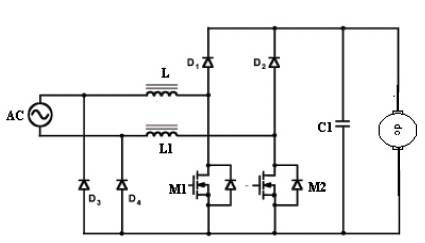
Figure 1. PFC Boost Rectifier with two diode
In this paper, a systematic review of bridgeless Power Factor Correction (PFC) boost rectifiers, also called dual boost PFC rectifiers, is presented. Simulation and analysis of bridgeless converter with motor load with its various performance characteristics are provided.
To meet the challenges of everincreasing power densities of today's ac/dc power supplies, designers are continuously looking for opportunities to maximize the power-supply efficiency, minimize its component count, and reduce the size of components. Recently, in an effort to further improve the performance of the front-end PFC rectifier, many power supply manufacturers and some semiconductor companies have started looking into bridgeless PFC circuit topologies. Generally, the bridgeless PFC topologies, also referred to as dual boost PFC rectifiers, may reduce the conduction loss by reducing the number of semiconductor components in the line-current path. So far, a number of bridgeless PFC boost rectifier implementations and their variations have been proposed [1]. In this paper, a systematic review of the bridgeless PFC boost converterfed DC drive is presented. Performance characteristics are studied.
So far, a number of bridgeless PFC boost rectifier implementations and their variations have been proposed [2]–[23]. In this paper, a systematic review of the bridgeless PFC boost rectifier implementations that have received the most attention is presented. Performance comparison between the conventional PFC boost rectifier and a representative member of the bridgeless PFC boost rectifier family is performed. Loss analysis and experimental efficiency evaluation are provided.
The basic topology of the Proposed PFC converter is shown in Figure 1. PFCs reshapen the distorted input current waveform to approximate a sinusoidal current that is in phase with the input voltage. There are several effective techniques for achieving a sinusoidal input current waveform with low distortion. Two typical techniques for PFCs are passive correction and active correction. In this study, only the single-phase input circuitry is considered. Passive PFC techniques shape the input current waveform by using a passive input filter consisting of inductors and capacitors. Because it operates at the line frequency of 50Hz, passive filters require relatively large fixed-value inductors and capacitors to reduce the low frequency harmonic currents. These filters use resonant pass or resonant trap circuits sensitive to both frequency and load. It is difficult to achieve near unity power factor with passive filters. Also, very large currents may circulate in the filter. However the passive filter is an effective PFC solution in cases where the line frequency, line voltage and load are relatively constant. An active PFC performs much better and is significantly smaller and lighter than the passive PFC circuit. The active PFC circuits operate at a higher switching frequency than the line frequency to allow a large reduction in the size and cost of passive filter elements. Their function includes active wave shaping of the input current, filtering of the high frequency switching, feedback sensing of the source current for waveform control and feedback control to regulate output voltage. Buck, boost, fly back and other converter topologies are used for the active PFC circuits. The boost circuit-based PFC topology is the most popular and is employed in this study. The boost PFC circuit is an economical solution to comply with the regulations. It can be implemented with a dedicated single chip controller, making the circuit relatively simple with a minimum number of components. Theboost inductor in the boost PFC circuit is in series with the ac power line. Therefore the input current does not pulsate minimizing conducted EMI at the line. This allows the size of the EMI filter and the conductors in the input circuit to be reduced. This topology inherently accepts a wide input voltage range without an input voltage selector switch. The output voltage of a boost PFC circuit should be higher than the peak value of the maximum input voltage. Although this is a simple topology, it must be designed to handle the same power as the main power converter. Only the single-phase boost PFC circuit operating in the continuous inductor current mode is discussed.
Figure 1. PFC Boost Rectifier with two diode
In Figure1, in addition to diodes D1 and D2 , which are slow recovery diodes, a second inductor is also added, resulting in two Dc/Dc boost circuits, one for each half-line cycle. During a positive half-line cycle, the first Dc/Dc boost circuit, L-D1 –M1 is active through diode D4 ,which connects the Ac source to the output ground. During a negative half-line cycle, the second dc/dc boost circuit, L1 –M2 –D2 , is active through diode D3 ,which connects the ac source to the output ground. It should be noted that switches M1 and M2 ,in bridgeless PFC boost rectifiers in Figure.1 can be driven with the PWM signal, which significantly simplifies the implementation of the control circuit. The drawback of the bridgeless PFC boost rectifier in Figure 1 is that it requires two inductors. However, it should also be noted that two inductors compared to a single inductor have better thermal performance.
The input power factor is defined as the ratio of real power over apparent power as
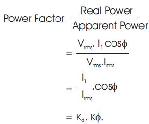
Where Vrms is the ac input rms voltage, Irms is the ac input current,I1 is the fundamental component of Irms and cosΦ is the phase angle between input ac voltage and the fundamental current, Kd is the distortion factor and KΦ is the displacement factor. Kd is the ratio of fundamental rms current I1 rms to total rms current. KΦ is the cosine of phase angle between input ac voltage and fundamental current. The input rms curernt Irms is expressed as
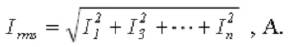
Where In is the nth rms harmonic current.
Based on the current and voltage ratings of switch, diode and passive components, the loss equations are derived. The PFC stage is at least rated to the maximum input power rating of the DC drive system given by
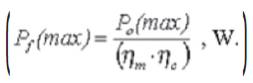
where Pf (max) is the maximum power rating of the PFC stage, Po (max) is the maximum output power of the DC drive system, ηm is the efficiency of the motor and ηc is the efficiency of the corresponding converter. The peak input current occurs at the minimum input line voltage with the maximum output power. The peak input current is expressed as,
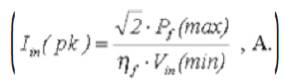
where nf is the efficiency of the PFC stage. The current flowing through each diode is a half-wave rectified sine wave. Therefore the average current through each diode is
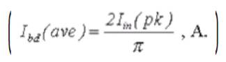
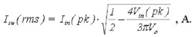
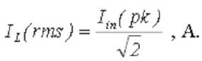
And the minimum voltage rating for the input rectifier diode is Vpk in (max). The minimum voltage rating of the boost switch is the output voltage of the PFC stage. The peak current rating is the same value as in the input rectifier bridge diode case shown in equation (4). The rms boost switch current is expressed as
The minimum voltage and current ratings of the boost diode have the same value as in the boost switch case. The rms current of the boost diode is given by
The inductor value is based on the current ripple in the boost inductor, which is usually chosen as a fraction of Iin(pk). The inductance value is expressed as,
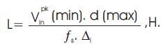
where Vpk in (min) is the peak minimum input voltage, fs is the switching frequency, Di is the ripple current and d(max) is the maximum duty cycle expressed as,
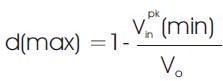
Vo is the output voltage. The rms boost inductor current is expressed as
The output capacitance for a given output voltage ripple is obtained by integrating the charging current into the capacitor over the entire switching period. The output capacitance is,
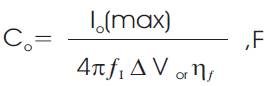
where Io (max) is the maximum output current, f1 is the line frequency and ΔVor is the output ripple voltage. The derivation of switching and conduction losses of the major power components in the PFC pre-regulator is explained in this section. The obtained device ratings and duty cycles are summarized in Table 1. The loss equations for major power devices are derived based on ratings and duty cycles and listed in Table 2. The switching loss is estimated with considering turn-on and turn-off transients of the switching device since both the maximum voltage and current are applied to the device during these incidents. The switching loss equation is derived under the assumption of the overlapped area by the maximum voltage and current as a triangular waveform.
where
Vfb =forward voltage drop of the inpuPt bridge rectifier, V
VCE (sat) = collector-to-emitter saturation voltage of IGBT switch, V
Rds (on) = drain-to-source on-resistance of MOSFET switch, Ω
tr = rise time of switch device, s
tf = fall time of switch device, s
Vf = forward voltage drop of power diode, V
trr = reverse recovery time of power diode, V
Rdc = dc resistance of inductor, Ω
The hardware for PFC fed drive is fabricated and tested. The experimental setup is shown in Figure 2. The pulses required by the MOSFETs are generated using ATMEL 89C2051 Microcontroller Oscillogram of driving pulses for M1 and M2 are shown in Figure 3. These pulses are amplified using the driver IC IR2110. AC input voltage is shown in Figure 4. Boost output is shown in Figure 5. The summary of speed with respect to the load is given in Table.3.the speed decreases with increase in load torque.
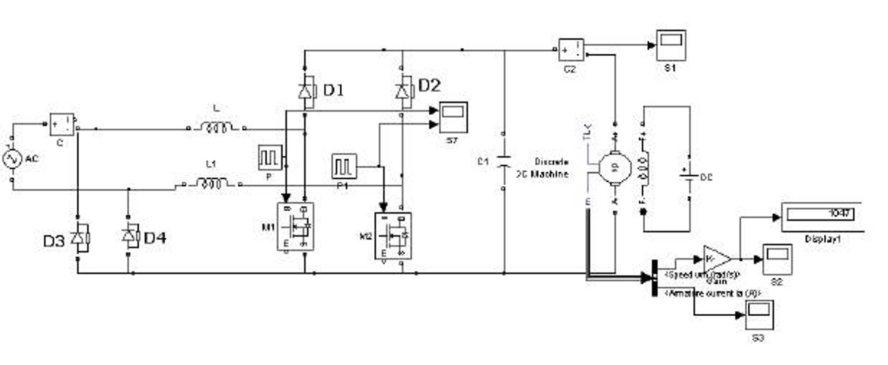
Figure 2. Proposed PFC Converter
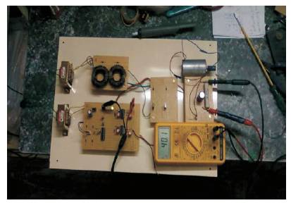
Figure 3. Experimental set up

Figure 4. Driving Pulses fo MOSFET
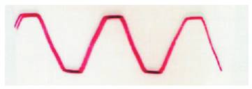
Figure 5. AC Input Voltage

Figure 6. Boost Output
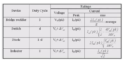
Table 1. Ratings for Power Components in the boost PFC Prergulator.
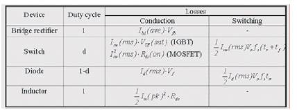
Table 2. Losses for Power Components in the Boost PFC Prergulator
The bridgeless PFC boost rectifiers, also called the dualboost PFC rectifier with motor load is simulated and their performance characteristics are studied. The efficiency of the front-end PFC stage is improved by eliminating one diode forward-voltage drop in the line-current path. The basic bridgeless PFC boost rectifier is not a practical solution because it has significantly larger common mode noise than the conventional PFC boost rectifier. The Simulation result is in line with the predictions.