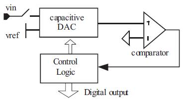
Figure 1. Block Diagram of a Typical Single-ended SAR ADC
A 10-bit single-ended ultra-low-power Successive Approximation Register ADC with a novel DAC switching technique is designed in the TSMC 0.18μm mixed-signal CMOS technology. This method uses a reference voltage of VR /2, rather than VR , as the only reference voltage to digitize the input signals with the amplitude range of [0, VR ]. Compared with the conventional switching method, this work reduces the size of binary-weighted capacitor array by 50%, lowering the average power consumption in the DAC during digitizing by 87.5%, and it also reduces the power consumption during sampling by 63.5%. With the sampling frequency of 77 kHz, ADC's post-layout simulation resolution is 8.84 bits and ERBW (Effective Resolution Bandwidth) is 60 kHz, and the post-layout simulation FOM of our 10-bit SAR ADC can reach 18.9 fJ/ (conversion-step), which is among the best ADCs FOM reported in a CMOS 0.18 μm technology
Successive Approximation Register Analog-to-Digital Converters (SAR ADCs) [1] are capable of providing very low power consumption, with medium-to-high-resolution and medium-speed for data conversion [2, 3]. As Figure. 1 shows, a single-ended SAR ADC mainly includes a capacitor array, a comparator, a digital control logic block and a sample-and-hold switch. A traditional comparator includes a pre-amplifier and a latch. Capacitor array and digital control logic block consume dynamic power, while the comparator generally consumes static power in the pre-amplifier and dynamic power in the latch. The size of digital logic is linearly dependent on the ADC resolution; however, the size of the binary-weighted capacitor array roughly doubles with an increase of each bit.
In recent years, several techniques have been applied to reduce the power consumption in the capacitor array. For example, one can
Each of the above proposed methods has their limitations. For example, the accuracy of the capacitor array using the attenuation capacitor will depend on the accuracy of the attenuation capacitor itself. The method of charging capacitor array via several interim voltages would not adversely influence the accuracy of the capacitor array, but the generation of interim voltages always needs additional circuits and consumes extra power, so the number of interim voltages in practice cannot be large (normally 2 or 3). The method of recycling charges stored in the capacitor array reduces power consumption when input signals are small, but it brings the penalty of nearly doubling the number of switches needed. The three-level capacitor switching scheme using three reference voltages (GND, Vref , and Vcm ), rather than two reference voltages (GND, Vref ), would consume power to generate the additional reference voltage. Furthermore, an ADC with three reference voltages suffers from the linearity issues while that using two reference voltages naturally does not.
In this paper, a SAR ADC with a novel low-power and areaefficient method to switch the capacitors in the DAC is proposed. Section 1 describes the structure and working flow of the proposed switching method. Section 2 demonstrates MATLAB simulation results of 6-bit DACs with different switching methods on power consumptions during digitizing and sampling, and SPICE simulation results on a 10-bit ADC with proposed DAC switching method in a single-poly, six-metal TSMC 0.18μm mixedsignal CMOS process using Cadence Spectre are shown in Section 3, which has been recently taped out. We will conclude the paper in Section 4.
Figure 1. Block Diagram of a Typical Single-ended SAR ADC
Initially, all capacitors in the capacitor array of a traditional SAR ADC sample input signal, and then under the digital circuits' control the capacitor array operates as a DAC to generate a set of intermediate voltages to gradually approach the sampled input signal, as shown in Figure 2 The comparator compares each intermediate voltage with the sampled input signal and outputs the corresponding bit. Based on the comparator's output, the digital logic controls the switching of the next capacitor to get the next intermediate voltage. Steps are repeated until the LSB is obtained.
As Figure 2 shows, DAC's initial intermediate voltage is GND. At the first digitizing step, it increases by VR /2 to compare with the sampled input signal to generate the MSB. If the sampled signal is larger than VR /2, MSB is equal to '1' and the intermediate voltage remains VR /2; else, MSB is '0' and the DAC's intermediate voltage returns to GND. The operation of the next step is similar, except that the step size is VR /4 rather than VR /2. From Figure. 2, we can see that digitizing voltages are [2-1 , 2-2 , 2-3 , 2-4 …2-N ] .VR , The largest digitizing voltage is in the first step and equals to VR /2. Based on aforementioned analysis, we present our novel switching method which uses one reference voltage of VR /2, rather than VR . In the proposed switching method, the largest digitizing voltage, VR /2, is the reference voltage, and the other digitizing voltages, [2-2 ,2-3 , 2-4 …2-N ] .VR , are generated from the only reference voltage, VR /2. Since all digitizing voltages are from the same reference voltage, VR /2, the linearity of SAR ADC is dependent on capacitors matching.
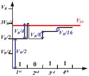
Figure 2. The flow of Digitizing a sample in a Traditional SAR ADC (red thick line: Sampled input voltage; black thin line: DAC's Intermediate Voltages).
Figure 3 shows the block diagram of the proposed capacitor switching method used in a binary-weighted capacitor array. The capacitor array is connected to the positive input of a comparator, and its negative input can be connected to either GND or the reference voltage, VR /2, depending on the value of MSB. If MSB is '1', which means VIN > VR /2, the comparator's negative input is connected to VR /2; if MSB is '0', which means VIN > VR /2, the comparator's negative input shall be connected to GND. The bottom plate of each capacitor in the array can be switched between GND and the reference voltage, VR/2, depending on the control signal from the digital control logic.
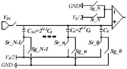
Figure 3. N-bit capacitor array with the proposed DAC switching method; “Sr_n”: switch controlling the connection of the capacitor corresponding to the nth bit to VR/2; “Sg_n”: switch controlling the connection of the capacitor corresponding to the nth bit to GND. During sampling, all capacitors are biased on VR/2.
A 2-bit SAR ADC is used as an example to explain how the proposed switching method works. Main steps include sampling input signals, generating 1st bit, and switching the largest capacitors to generate 2nd bit.
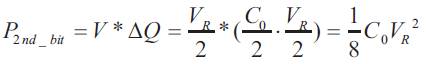
As Figure 4 shows, at first, all capacitors' top plates are connected together to sample the input signal while all bottom plates of all capacitors are biased on VR /2. Subsequently, the capacitors' top plates are first disconnected from the input signal and keep the sampled voltage. The sampled input signal enters the comparator via the positive input to compare with VR /2. If VIN < VR /2, MSB is “0” and the comparator's negative input is switched to GND. If VIN > VR /2, MSB is “1” and the comparator's negative input is still VR /2. In the generation of MSB, there is no capacitor to move and therefore ideally no power consumption in the capacitor array. In the 2nd bit generation, the largest capacitor in the capacitor array C0 in this 2-bit SAR ADC is switched to GND, and the voltage at the capacitor's top plates becomes VIN -VR /4. In the case of VIN < VR /2, as Figure 4 (c) shows, VIN - VR /4 is compared with GND. If VIN >VR /4, digital output is “01”; otherwise, the digital output is “00”. In the case of VIN > VR /2, as Figure 4(d) shows, VIN -VR /4 is compared with VR /2. If VIN >3VR /4, digital output is “11”; otherwise, the digital output is “10”. In the generation of the 2nd bit, the energy can be estimated as:
For our N-bit SAR ADC, the first two bits are generated as shown in the example of the 2-bit SAR ADC in Figure 4. The generation of the following N-2 bits is almost the same as that with the traditional switching method. The only difference is that in our proposed switching method, capacitors in the capacitor array switch between VR /2 and GND while in traditional capacitor switching method, the capacitors switch between VR and GND.
There are also several other features of our proposed novel SAR ADC design:
With the proposed switching method, when the amplitude range of input signals is [0, VR ], the needed reference voltage is VR /2. If VR >VDD, the reference voltage VR /2 can be readily generated on-chip. In the advanced nanometer CMOS technology with a sub-1V VDD, the generation of on-chip reference voltage is typically based on a current-mode method of scaling down the band-gap reference voltage by a factor defined by a resistor ratio. It is therefore easier to generate this lower VR /2 voltage on-chip for our proposed SAR ADC. Also, since VR /2 is half of the amplitude range of the input signals, if this proposed SAR AC uses power supply as reference voltage VR /2=VDD, it should be able to digitize input signals with amplitude range of [0, 2VDD].
From a system perspective, the reduction of a SAR ADC's input capacitance can decrease the required driving current for the previous stage, consequently reducing the power consumption in the previous stage and in the overall system.
If we assume the input signals are evenly distributed in the range [GND, VR ,], with the traditional switching method the energy consumed in the previous stage to charge the capacitor array during sampling is C .V2IN , where C is the total input capacitance of the SAR ADC. For a clear comparison, integrating energy over the whole input range, we will get:
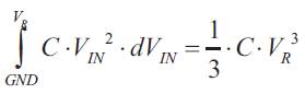
With our proposed switching method in the capacitor array, the sum of energy consumed in the previous stage during sampling is:
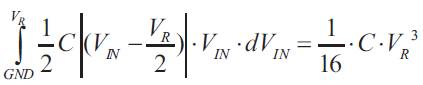
since the capacitor size with the proposed switching method is half of that with the traditional switching method. From the above calculations, our proposed switching method can reduce the power consumption in the previous stage by 82.25% vs. that with the traditional switching method, and it also decreases the required driving current of the previous stage by 75%. However, unlike the traditional SAR ADC design, please note that with the proposed switching method, the reference voltage VR /2 need to consume power during the sampling of input signals. The sum of energy provided by the reference voltage, VR /2, during sampling is:
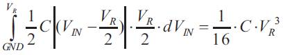

Figure 4. The Working Flowchart of the Proposed Capacitor Switching Method in the Capacitive DAC for a 2-bit SAR ADC: (a) Sampling input; (b) Directly Comparing to Generate 1st bit; (c, d) Switching of the Largest Capacitor for the 2nd bit Generation.
A MATLAB program is used to build up models of power consumption in the capacitor arrays to compare the traditional switching method and the split switching method against our proposed DAC switching method [4]. Figure 5 shows the energy consumed during digitizing in these capacitor arrays with different switching methods. The sum of energy consumed of each output code with the traditional method is 2667 C0VR2, while that with the split switching method is 1675 C0VR2, and that with our proposed method is only 325.5 C0VR2 (~1/8 of that with the traditional method). This is basically because: (1) the capacitor array's size is reduced by half with the proposed switching method; and (2) furthermore, the capacitors in the array with the traditional method are charged by V , R while they are charged only by VR /2 with our proposed method.
Figure 6 shows the energy consumed in the DAC during sampling. Capacitor arrays with either the traditional method or with the split method will consume the same energy of ~1365 C0 V2R , so they overlap in Figure 6 (note the capacitor size and reference voltage are the same for both methods). Energy consumed by the capacitor array with our proposed method includes two parts: one part is from the input signal and equal to 256 C0 V2R , and the other is from the reference VR /2 and it also equals to 256 C0 V2R .This is because the capacitor array with our proposed switching method is biased at VR /2, rather than GND, during sampling of the input.
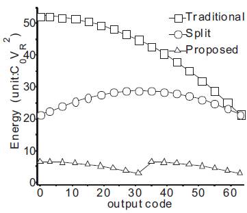
Figure 5. Matlab Simulation on Energy Consumed During Digitizing in the DAC with Different Switching Methods.
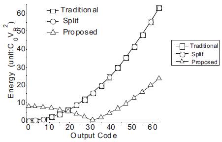
Figure 6. Matlab Simulation on Energy Consumed During Sampling in the DAC with Different Switching Methods.
The pre-layout simulation and post-layout simulation results of the 10-bit SAR ADC are summarized in Table 1. The main reason why the resolution in post-layout simulation is about 1 dB less than that in pre-simulation is that parasitic capacitance influences the accuracy of binary-weighted capacitance array and that the singleended ADC's resolution is limited by sample-hold switches. Figure 7 shows the simulation results of the differential nonlinearity (DNL) and integral nonlinearity (INL) of the proposed SAR ADC. Figure 8 shows the FFT spectrum analysis. The 2nd harmonics of the input frequency is clearly seen as the ADC is single-ended. The full layout is shown in Figure 9.
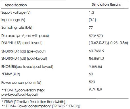
Table 1. Summary of the SPICE Simulation Results of the Proposed 10-bit SAR ADC
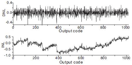
Figure 7. Simulated DNL and INL (unit: LSB)
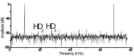
Figure 8. Simulated 1000 point FFT spectrum at fs=77 kHz and with input tone at 9 kHz for the proposed 10-bit SAR ADC
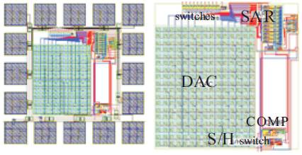
Figure 9. The layout of the proposed 10-bit SAR ADC (LEFT) with a zoom-in view (RIGHT)
The proposed switching method for the capacitor array in a SAR ADC uses the only reference voltage of VR /2, rather than VR , to digitize the input signal with an amplitude range of [0, VR ]. Reference voltage of VR /2 is used as the largest digitizing step, and the other digitizing steps, [2-2 , 2-3 , 2-4 …2-N]•VR , are generated by the binary-weighted capacitor array and VR /2. Consequently, compared with the traditional switching method, the proposed capacitors' size is reduced by half, power consumed in the previous stage to charge capacitors during sampling is reduced by 81.25% and the power consumed from the reference voltage to charge the capacitor array during digitizing is also reduced by 87.5%. Furthermore, with this proposed method, the linearity performance is not influenced, and the SAR ADC can digitize signals larger than the power supply. A 10-bit single-ended SAR ADC with novel lowpower and area-efficient switching method in the DAC is therefore designed and laid out in the TSMC 0.18μm mixed-signal CMOS process. With the sampling frequency of 77 kHz, the simulated FOM can reach 18.9 fJ/(conversion step), which are among the best ADCs reported in CMOS 0.18 μm technology.
The authors thank their team members for their kind support. The authors are also indebted to the funding support from the Semiconductor Research Corp. (SRC) through the Texas Analog Center of Excellence (TxACE) Center.